Hi everyone, I need some assistance with this simple 50watt class AB I copied from a kit. I powered it up and get app 3.7v at the midpoint which should read app 1/2vcc or 25v as I am testing it with a 50v supply. I have adjusted the bias current via vr1 to app 40Ma
Attachments
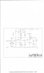
This is a very old circuit, based on a mediocre RCA design of the 70's, with mediocre performance. Your T2 is shown as BC337. That is only rated to 45V, and should not be used in this position. You ought to use a 60 or 80V (or higher) voltage transistor, such as BC546 or maybe 2N5551. I suspect the one you have may be dead (shorted), so check this first.
Last edited:
Nice work. As an initial suggestion, have look and check that the orientaion of the transistor connections is right - that's easy to confuse when planning a layout or using a breadboard/matrix board assembly. Note that some brands of TO92 transistors have different pinouts to others, even though identical in appearance. Check the datasheets.
Then check the Vbe of all transitors, powered up, with no load or input.There should be an approx. 0.65V diode voltage across the base and emitter of all bipolar transistors. Naturally, the polarity will be reversed for NPN or PNP type. Happy hunting")
Then check the Vbe of all transitors, powered up, with no load or input.There should be an approx. 0.65V diode voltage across the base and emitter of all bipolar transistors. Naturally, the polarity will be reversed for NPN or PNP type. Happy hunting
Thanks John, I have adjusted R3 and have got the midpoint at exactly half Vcc. Next thing is to figure out why my gain is so low I am injecting 1khz at app 600mV and only getting 4.7v out. I would have thought it would be R15/R2 that would set the gain. I have replaced both the 337 with 546.
No, epicyclic said what controls the gain. But R15 and R2 provide feedback which is shunted by C2. Normally C2 grounds the AC signal, so these work at DC to low frequencies, but if you left that out it would reduce the gain.
Or if your feedback resistor R6 is the wrong value the gain could be low. Or the input resistor too high. Check R1, R6 and C2 and the whole feedback loop.
You might also check you have got the transistor leads the right way round. I doubt that T2 would be a problem as you set the centre rail OK but if T1 were upside down it would limit the gain.
Last edited:
Three ways to reduce the distortion in this no-so-golden oldie:
1. The biggest contribution to distortion is crossover. So change the output to complementary using TIP3055 and TIP2955 pair. Preferably matched, along with matched drivers. The bias stabiliser will need to be changed. You can add another diode or preferably replace the diodes and resistor with a Vbe multiplier. Use only a single resistor between the bases of the output transistors rather than separate base resistors to the output rail.
2. If you can tolerate a lower overall gain, remove the 390k feedback resistor and C2 and use only R15-R2 feedback to increase overall negative feedback. Gain will be around 20 instead of 39.
3. Somewhat riskier, change the compensation capacitor connection to the mid-rail (output) rather than collector of T2. That speeds up the pre-driver (VAS in modern terminology) and helps to reduce crossover. The risk is that the amplifier may oscillate, in which case you can either reconnect it in the original position or add a 100pf- 100 ohm damper network across the collector of T2. Though I have not found a problem with this particular circuit.
Depending on the load, you may also, or instead of the damper, need to use the traditional LR/RC network on the output lead. As you already have the RC network this only needs a small coil (10-20 turns usually, on a 10mm dia non-conductive tube) in parallel with a 4.7 or 10 ohm resistor. Sometimes people have wound the coil on the resistor. Wire dia. needs to be suitable for the current (e.g. 0.7mm copper dia). This is wired in series with the load, after the RC network. So my preference is to add the LR network which should suppress RF getting back into the amplifier which directly connecting a feedback capacitor could do.
Sorry this is not so simple an amp. now, but the old circuits more or less became extinct decades ago.
But they worked back then and still work (as well or not) now.
Last edited:
I have another problem the ac waveform appears at T6 base but there is no waveform at T5 base even if you adjust VR1 to max. The waveform appears at the base of T3 and the collector. The bias current is 45mA through T6 and T5. The voltage across R7 is 1.038v or app 3.8mA the voltage across R10 is 0.625v and 0.637v at R11. John you are right this is not as simple as it looks
Re: #11
Quasi-complementary amplifiers don't really have a consistent optimal bias level that you can demonstrate as the best or lowest THD level. Distortion tends to level out with about 15 mA bias current and perhaps is best at about 35 mA. The rest is determined by 'scope or by ear, depending on your pleasure. After all, you have an Emitter follower (EF) pair in cascode with a Sziklai pair (CFP) so it's unlikely that either will have optimum bias current when lowest THD or best sound quality is achieved.
Having said this, the temperature and thermal stability of the output stage can be a factor in bias setting. This is sometimes ignored until the smoke and swearing starts.
The usual bias current range for this amplifier is in the range 15-50mA. A simulation gives 0.76% THD at 15mA, 30mA 0.71% and 50mA 0.72%, at 1.3V out (100mW) so Ian's 35 mA seems about right. I haven't run a complete test to find the peak distortion for each bias current, but crossover tends to peak at 50-100mW. If you want to learn, get one of the free simulators and try this exercise!
There is something unusual with this circuit in that T1 and T2 are both NPN's.
I looked at the Quad 303 schematic as I knew this is an inverting amplifier this uses the usual complementary pair for the front end - which is the usual form for Lin amplifier derivatives.
Also the input supply divider network 18k/4.7k lacks a decoupling capacitor from the junction of the two connecting to earth.
If the problems being experienced are to be solved further detail of the kit whether the schematic or board overlay might be of help.
It is not common for both transistors to be NPN, but this is not unlike the emitter follower+VAS combination (without the PNP input transistor(s)). The consequence of having two non-linear elements in series is more non-linearity. Even after applying my suggested mods in post #9 the limiting distortion is around 0.15% which I suspect is due to this input arrangement. However, one advantage is that this configuration is quite stable.
Using a more conventional PNP-NPN stage would give lower distortion but then has the usual debate about how to stabilise it. With care a phase-lead capacitor gives a better transient performance than Miller, and is usually doable with just the two stages.
Using a more conventional PNP-NPN stage would give lower distortion but then has the usual debate about how to stabilise it. With care a phase-lead capacitor gives a better transient performance than Miller, and is usually doable with just the two stages.
Not really. T1 only has to remain "on", its collector voltage does not have to do anything as it is not part of the signal chain. As long as the voltage is greater than the saturation value (which would be the Vb of T2 plus about 0.25V, preferably 1V) then T1 will function properly. As T1 operates at about 800uA and the current supplied by R16 is about 2.5mA there is sufficient margin.
- Status
- This old topic is closed. If you want to reopen this topic, contact a moderator using the "Report Post" button.
- Home
- Amplifiers
- Solid State
- Simple circuit help