According to LTSpice the input stage's current source is very stable. With these simulations I am getting only a 1uA variation in its output current which translates to 1/3000.
The only current path besides the input stage's current mirror is through the differential pair's bases. However, current has to pass in the opposite direction to what it should under ordinary conditions. If this is true, the only reasonable conclusion is the differential pair's base-collector capacitance. This capacitance is being partially charged and discharged as a result of the rails artifacts and hum.
The only current path besides the input stage's current mirror is through the differential pair's bases. However, current has to pass in the opposite direction to what it should under ordinary conditions. If this is true, the only reasonable conclusion is the differential pair's base-collector capacitance. This capacitance is being partially charged and discharged as a result of the rails artifacts and hum.
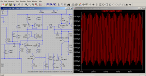
The mains hum, or better 100Hz buzz, can easily be seen in the attached screenshot. This was obtained by adding the cascode's emitter currents and subtracting the input stage's current source's Ic. Due to the negative sign of Ic, I had to use an addition. Nevertheless, this should be easily to grasp.
The amplitude of oscillations illustrated in the screenshot is the sum of base currents feeding into the differential pair's bases.
The golden question here is: Why am I getting a 100Hz signal superposed on the legitimate signal?
The amplitude of oscillations illustrated in the screenshot is the sum of base currents feeding into the differential pair's bases.
The golden question here is: Why am I getting a 100Hz signal superposed on the legitimate signal?
Attachments
Last edited:
The 30 minutes edit time expired. So, I will have to post here:
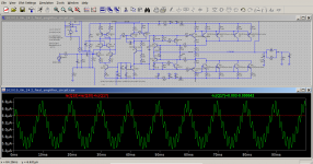
The second screenshot shows the difference between the cascodes' emitter currents and the current mirror's Ic. These almost cancel out. The green trace is the current mirror's Ic. The modulating mains buzz is clearly illustrated.
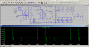
The third screenshot shows the difference between the cascode's Ics. There are spikes in synchrony with the start and end of smoothing capacitor charging.
The second screenshot shows the difference between the cascodes' emitter currents and the current mirror's Ic. These almost cancel out. The green trace is the current mirror's Ic. The modulating mains buzz is clearly illustrated.
The third screenshot shows the difference between the cascode's Ics. There are spikes in synchrony with the start and end of smoothing capacitor charging.
I have just discovered that with the differential inputs shorted together, the VAS does not work properly, and is heavily out of balance. This, unfortunately, invalidates all these latest simulations.
To Moderators:
I would greatly appreciate if a moderator with post deletion power removes my latest posts from post #575 onwards.
Thanks.
To Moderators:
I would greatly appreciate if a moderator with post deletion power removes my latest posts from post #575 onwards.
Thanks.
To Moderators:
I would greatly appreciate if a moderator with post deletion power removes my latest posts from post #575 onwards.
Thanks.
I know you'll understand
") We don't normally edit threads/posts, particularly where replies have come in in response to content already posted.
We don't normally edit threads/posts, particularly where replies have come in in response to content already posted.A thread is like a timeline, it tells a story and so to delete posts isn't really fair on those who have replied or on those who are following.
Your thread shows the design processes at work... and that is what it is all about.
As previously stated star earth schemes are not easy to implement. There is a brief article on this at https://www.edn.com/design/consumer/4429968/The-G-word--How-to-get-your-audio-off-the-ground.
Given the persistence of your problem it would be worth paying the money to get the full articles. I have run a Tian simulation test which shows you have ample phase and gain margins even if your Miller capacitor is reduced from 100 pF to 39-47 pF.
Such reduction is made possible because the closed loop gain is 56.55 which places the unity gain point at 244 kHz which is very low by most standards.
There is about 3dB of mound of base boost below 100Hz which is rather strange.
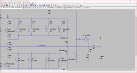
I have attached the symbols and connections for a Tian plot so you can do your own investigations on your latest update of the simulation.
To use this you have to replace the expression for Vout with -1/(1-1/(2*(I(Vi)@1*V(x)@2-V(x)@1*I(Vi)@2)+V(x)@1+I(Vi)@2)) by clicking on that header in the plot. I usually copy this and put it at a convenient space on the .asc file and change the status from SPICE directive to Comment.
Select the two cursor option and drag one to 0 dB using the side arrow keys for fine adjustment Do do likewise for the second cursor placing this as close as possible to -180 degrees. Read off the stability margins in the box at the bottom.
Given the persistence of your problem it would be worth paying the money to get the full articles. I have run a Tian simulation test which shows you have ample phase and gain margins even if your Miller capacitor is reduced from 100 pF to 39-47 pF.
Such reduction is made possible because the closed loop gain is 56.55 which places the unity gain point at 244 kHz which is very low by most standards.
There is about 3dB of mound of base boost below 100Hz which is rather strange.
I have attached the symbols and connections for a Tian plot so you can do your own investigations on your latest update of the simulation.
To use this you have to replace the expression for Vout with -1/(1-1/(2*(I(Vi)@1*V(x)@2-V(x)@1*I(Vi)@2)+V(x)@1+I(Vi)@2)) by clicking on that header in the plot. I usually copy this and put it at a convenient space on the .asc file and change the status from SPICE directive to Comment.
Select the two cursor option and drag one to 0 dB using the side arrow keys for fine adjustment Do do likewise for the second cursor placing this as close as possible to -180 degrees. Read off the stability margins in the box at the bottom.
Attachments
Pasting the given expression and pressing OK, displayed a dialog complaining: "Invalid @step resquest" and "This data does not contain steps".
Sorry but had a commitment to attend to this morning and in a hurry to finish that last post. You need these commands copied in two blocks - I have attached a text file to make it easier to copy these into your simulation.
Code:
.options numdgt=15
.param Freq=2k
.param numcyc=80
.param dlycyc=5
.param FFT=2**16
.param simtime=numcyc/Freq+dlytime
.param dlytime=dlycyc/Freq
.param timestep=(simtime-dlytime)/FFT
.four {Freq} V(Vin) V(Vout)
.four {Freq} 4 V(Vin) V(Vout)
;
;tran 0 {simtime} {dlytime} {timestep}

.option numdgt=15

.option reltol=1e-6
.option ptrantau=0
;
.ac dec 500 1 10g

and

.step param prb list -1 1 ; set prb=0 to turn off probe
;.par prb=0
Attachments
Added the two lists of commands and parameters. Processing took around 20 minutes to complete. Pasting "-1/(1-1/(2*(I(Vi)@1*V(x)@2-V(x)@1*I(Vi)@2)+V(x)@1+I(Vi)@2))" in the plot window selector, I got a Power (KW) vs time graph. The LTSpice error log contained the error "Unknown parameter 'u'".
You have some prescriptions for monitoring heat in the driver and output transistors and increase in power dissipation that are not taken into consideration as a stability issue as far as gain and phase margins are concerned in this simulation approach. I dispensed with these and used standard .models for the drivers and outputs. You could replicate the effects on heat increase and power dissipation by manipulating the output current. You still have C10 at 1uF loading the output be aware the phase and gain margins will look worse. This is pretty much worst case testing but if the gain declines to unity before the phase reaches -180 degrees say -155 it should not be going to get any worse. I have not seen any simulation with this loading and removed it in mine to give a conventional result - you might like to do some research in that regard.
With a 10R resistor splitting ground into two parts, namely, signal ground and power ground, I would like to be sure which 'ground' should be connected to signal outer shielding. By 'shielding', I am referring to the multitude of fine copper strands, that surround the inner insulated wire. I have always connected this sheilding to the sound source signal ground.
The input PCB contains four input sockets: two XLR females which are completely insulted, and two large phone females with the ground in contact with the amplifier metal box. The latter, in theory, can create an alternative current path for ground currents inside the amplifier box. However, for this to be possible the box's insulating paint must be scratched. Microscopic scratches are a possibility that I cannot exclude. My intuition tells me, this second unwanted internal ground path, must have a high resistance, but I may be wrong as I lack experience in grounding sensitive electronic equipment.
The second ground path can be eliminated by making a new PCB instead of using the original input PCB and by removing the two large phone females.
Keep in mind that the current gain of BJTs drops with increasing frequency. If you have some Transistor with current gain 100 and a transit frequency of 100MHz - the current gain at 1MHz is something like 70, decreasing with 6dB/oct reaching unity at 100MHz.Self Oscillations Demystified:
So far, I learnt a bipolar transistor always present an emitter-base capacitance albeit extremely small. This small capacitance is effectively in series with the input resistance and forms a low pass RC filter. The useful signal is across the capacitor, which means, as the input frequency is increased, the voltage across the capacitor will eventually cease to cause any current to flow through the base-emitter region.
With reduced current gain the base current rises with frequency reducing input impedance accordingly. This is what looks like an input capacitance - but explains real effects that cannot be explained by the tiny input capacitance.
<snip> The second ground path can be eliminated by making a new PCB instead of using the original input PCB and by removing the two large phone females.
You must have only one ground connection. You can buy phono sockets with insulating washers so these don't come into contact with the chassis. It is not hard to ream out holes to allow these to fit.
If you have pcb mount types one would have thought it possible to find some simple way of isolating them.
If you have non-insulated input sockets, you can minimize grounding issues by mounted them on a reasonable thickness of aluminium or copper plate which is itself the grounding point. 3mm thick Al plate has a resistance of about 10µohm/square, which will reduce the effects of pretty large ground currents substantially!
Of course this cannot correct for resistance of cables, but you can match all your inputs together well by the chassis.
Compare with PCB groundplane which is 0.5mohm/square, or a thin steel chassis
Of course this cannot correct for resistance of cables, but you can match all your inputs together well by the chassis.
Compare with PCB groundplane which is 0.5mohm/square, or a thin steel chassis
Last edited:
The phono chassis sockets are not on the schematic for the original equipment which shows XLR sockets. We have been informed these are insulated types. The equipment was designed for professional use.
There is only one choice as to which of these two input schemes is correct.
There has been some recent controversy about that see How to wire up an Amplifier for your possible options.
There is only one choice as to which of these two input schemes is correct.
The question here is where does the earth end of R14 connect.With a 10R resistor splitting ground into two parts, namely, signal ground and power ground, I would like to be sure which 'ground' should be connected to signal outer shielding. By 'shielding', I am referring to the multitude of fine copper strands, that surround the inner insulated wire. I have always connected this sheilding to the sound source signal ground.
There has been some recent controversy about that see How to wire up an Amplifier for your possible options.
The phone females at the back panel are of the type commonly used for earphone outputs. Mobile phones, laptops and portable mp3 players usually have them. The male plug is like a long tapering finger with multiple insulated rings along its length. One can find such males with two, three and even four rings.The phono chassis sockets are not on the schematic for the original equipment which shows XLR sockets. We have been informed these are insulated types. The equipment was designed for professional use.
The following link shows the small male version. Please, note the back panel does not have males, but females.
Amazon.com: NAC Wire and Cables Audio Phone Plug 1/4" Stereo 6.3mm Plastic Handle Metal Threaded Insert Solder Terminals Strain Relief Design Threaded Insert Black Plastic Handle 1/4" Stereo Audio Phone Plug,: Electronics
- Home
- Amplifiers
- Solid State
- My attempts at a design of a 3 stage amplifier