That means somehow telling LTSpice to simulate for the output resistance suddenly becoming infinite. I do not know how to instruct LTSpice to do that.mjona said:So what happens if a voltage spike is generated across the output transistors when an attempted termination of output current occurs at high power outputs?
That means somehow telling LTSpice to simulate for the output resistance suddenly becoming infinite. I do not know how to instruct LTSpice to do that.
As you appreciate when the output transistor current is terminated the speaker coil is still in motion there has to be a discharge path for the electrical energy generated by this at high power.
Where I see this heading is you will need to specify all your component designations in order for someone to upload that detail into software for circuit board layout. I don't build amplifiers of this scale and design my layouts by hand.
The usual way to divert spikes is to connect rectifier diodes in reverse polarity to the supply rails between these points and the amplifier output.
If you look inside your hardware you will see the evidence of this.
I don't include this sort of detail on my .asc files and deal with this when I draw up the circuit board.
You have not covered this base in your simulations - don't be caught unawares.
Thank you for your advice. Yes, I noticed two diodes across the NPN and PNP transistor arrays, but I did not know what was the purpose. I thought it was to protect the output when there is a polarity reversal, although at these voltages such a thing would certainly cause some form of damage.
Like you, I will manually create the PCBs. The first will be two narrow PCBs for the NPN and PNP array sections. The other circuit parts will be on a large separate PCB.
Like you, I will manually create the PCBs. The first will be two narrow PCBs for the NPN and PNP array sections. The other circuit parts will be on a large separate PCB.
It seems it will be a real uphill struggle to make the PCBs! The good-old PCB tracks/pads transfers were too good for me. I tried several methods, and failed to produce a neat looking PCB in all of them. Using software seems like trying to learn to use a 100 ton excavating machine to dig 15cm holes to plant your vegetables! Why all these unnecessary complications for a single sided single layered PCB? I do not plan to use surface mount junk for obvious reasons.
This hurdle seems to be set too high for me. I have the circuit diagram together with a powerful power supply and a fine amplifier box, but with this horrible new so-called technology, I am unable to produce a decently looking PCB.
Sorry for my rant, but it is exasperating not to be able to do something, that used to be easy to the extent of being ready in a matter of two hours.
The new method is cumbersome to the extent that one has to wait for several days if not weeks to get some feedback as to whether used software in PCB production is adequate or not. Besides that, one has to fork good money for that!
Steady on there - time for a break perhaps.
You can get help from members who have skills with pcb layout. With a project like this one you might be looking at separate boards for a number of functions and you would have to pay for the work and you could easily need more than one prototype as the layout is part of the circuit not covered by simulations. The one you should be concerned for is the stability and to allow extra in your margins.
Your circuit development has gone a long way since any Tian plot has been posted.
I used to rely on simulations with 10kHz square wave into 8R// so many uF. In some instances where the outcome is favourable there is a problem when the uF element is reduced in value or taken away.
That is if the feedback loop is less stable at high frequencies a high uF value in parallel with a load can lower the resonance and give the impression of stability. Small values equate to higher resonance frequencies which can undo such results.
You don't want to find that sort of result when your hardware is bench tested.
I am using pcb-gtk which uses geda footprints and other footprints from other sources. There were no TO3PL footprints, so I searched for the TO126W footprint which exists and reversed engineer the code to convert it to TO3PL. Although, it seems, I was successful, I cannot make sense of the Mark(a b) statement. a and b are coordinates and Mark appears as a small slightly rotated square. I saved the TO3PL.fp to the directory where geda footprints are saved and pcb-gtk listed it and I could use it.
Since spending money is involved in ordering PCBs, I am very cautious and hesitant not to make mistakes.
With the TO3PL.fp footprint I can make the power stage's PCBs and order them, hopefully.
Since spending money is involved in ordering PCBs, I am very cautious and hesitant not to make mistakes.
With the TO3PL.fp footprint I can make the power stage's PCBs and order them, hopefully.
Does an electrolytic capacitor across the amplified diode protect a speaker from turn on plops?
No.
Find a circuit that uses a relay to delay connecting the amplifier to the speakers and in case of a dc output fault to prevent the risk of the amplifier from burning out the speakers with the possibility of starting a fire.
Works in progress... 
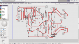
This is yet another PCB design. It is for the input, VAS and driver stages. These will be mounted on brass spacers fixed to the heatsink. Part of the original PCB will be used which houses the smoothing stage of the power supply and output transistor arrays. The unwanted original circuitry has been removed and the board real estate sawed off neatly. In its space the new PCB will be fixed.
I am attaching the PCB as it is displayed in pcb-gtk (Linux application).
P.S.
There is an error connection in the input. The shown input is connecting to the base of a cascode transistor, this is wrong. The connection should be to the base of the lower transistor. Patience, human beings get tired and make mistakes.
Attachments
Last edited:
PCB design isn't easy. One thing I have learned is that it pays to make pads and tracks as wide as possible. Those (default) pads will be awfully tiny in real life.
Have a look at post #22 to get an idea of how large I make pads.
GERMANIUM Single ended Class A Headphone Amp.
Have a look at post #22 to get an idea of how large I make pads.
GERMANIUM Single ended Class A Headphone Amp.
The signal tracks are 1mm wide and the pads can easily be enlarged. Yes, I noticed the default pad and track sizes are very small, too small for comfortable soldering.
At the moment, I am modifying the remainder of the original circuit to make it compatible with the new amplifier circuit and to implement a better thermal resilience.
The original circuit had one fuse on the 0V rail. The positive and negative rails were not fused. I think, a fuse on the 0V rail protects a speaker and in the event of blowing, the amplifier does not clamp to either the positive or negative rails. Simulations seems to confirm this. If this is the case, it seems to be better for me to keep the existing 20A fuse on the 0V rail. The posted schematic, the last one, may need the addition of two resistors across the +ve and -ve supply rails to create a virtual 0V rail. The current supplying the biasing for the constant current sources may need to be taken from between the +ve and -ve rails.
Last edited:
Working on the hardware.
a) remove the unwanted electronics from the original circuit
b) isolate the heatsink from the output transistors
c) move the output inductor and resistor, 2uH in parallel with 6.8 Ohms, from the 0V rail to the output rail
d) complete the feedback path for the complementary feedback pairs and change the 3.3 Ohm resistors to 0.1 Ohm.
In the original heatsink setup the output transistors were held in contact with the heatsink with a clip. I will remove that and use screws and insulators.
When I get ready, the output (without a VAS and input) will be stress tested for leakages. I will use the full 170V DC voltage for this but first I will connect a resistor in series with the circuit.
High power, 40W, 0.1 Ohm resistors.
From where can I find 0.1 Ohm resistors with a power of at least 40W? Are heatsink mounted resistors good?
I arrived at the 40W figure because there are 4 0.22 Ohm emitter resistors. Collectively these can be seen as 0.22/4 Ohms = 0.055 Ohms with a rating of 4x5W = 20W. Since our resistor is 0.1 Ohm, approx. double 0.055 Ohm, the required power rating should be 20W x 2 = 40W
You are saying that 0.1 Ohm resistors of this power are a rarity. But large amplifiers are manufactured every day all year round, therefore, there is something impractical in my design. My design simulates well, that is not enough. Using arrays of parallelised resistors to make up a large power 0.1 Ohm resistance is neither used.
Since keeping an amplifier stable is always an issue, I am coming to the conclusion, it is better to avoid having to use these large 0.1 Ohm resistors and stick to the original power stage. Yes, it will mean a complicated amplified diode with drastic temperature compensation, but that, is more accessible compared to a part that is not normally found in amplifiers.
Since keeping an amplifier stable is always an issue, I am coming to the conclusion, it is better to avoid having to use these large 0.1 Ohm resistors and stick to the original power stage. Yes, it will mean a complicated amplified diode with drastic temperature compensation, but that, is more accessible compared to a part that is not normally found in amplifiers.
A rarity in that I've never come across an amplifier with anything like that wattage of low value resistor fitted. Thinking more about this, when you are talking of these kind of current flows then the wiring/print becomes as much a dominant factor as does the value of resistor you want.
I searched for such resistors and found quite a few but I've never seen anything like these fitted in an output stage.
https://cpc.farnell.com/welwyn/wh50-0r1-ji/resistor-ww-50w-5-0r1/dp/RE03483
https://cpc.farnell.com/welwyn/wh25-0r1-ji/resistor-25w-5-0r1/dp/RE04699
https://cpc.farnell.com/welwyn/wh10-0r1-ji/resistor-ww-15w-5-0r1/dp/RE01648
TO3-PL transistor packages:
To securely mount the 2SA1943 and 2SC5200 power transistors onto the heatsink, I need to widen the transistors' holes to 4mm diameter. The diameter increase is 1mm. The plastic is some kind of very hard plastic.
Is this safe to do?
Don't do that use a smaller diameter bolt. There are sleeves with shoulders that come with mica washer sets.
Feed these through the hole in your transistors through to the reverse side of the heat sink and use washers to spread the load when tightening the bolt on the transistor side and on top of the shoulder of the sleeve insert on the other side of the heat sink where the nut is to be fastened.
If this is not enough then buy strips of 1 cm thick aluminium bar long enough to clamp the bodies to the heat sinks and wide enough to cover the black upper surface of the transistor bodies.
- Home
- Amplifiers
- Solid State
- My attempts at a design of a 3 stage amplifier