An additional comment about the resistance of the emitter diode is this is temperature dependent and the voltage drop across this is roughly 26 m.V. at room temperature taken as 25 degrees C or 298.15 degrees K. If the temperature increases the emitter diode resistor drop will decrease in proportion to new value on the Kelvin scale.
You could look at the driver transistors and the vbe transistor to see if you can get the temperature compensation right. I have not investigated this.
You could look at the driver transistors and the vbe transistor to see if you can get the temperature compensation right. I have not investigated this.
Last edited:
Nearing my aims. 
Features:
a) No ringing of driver base currents at 16kHz
b) Drivers and power output transistors thermally protected with the quiescent current almost remaining CONSTANT over the temperature range of 27C - 65C.
c) A distortion figure < 0.2% for ear-drum breaking powers.
d) A beautiful square wave at 20kHz
e) With the output filters, and assuming a parasitic capacitance of 1uF in the output, the phase angle of the output never reaches 180 degrees. This over the range of 10Hz - 100kHz.
f) The circuit uses the exact same output stage, so I do not need to remake it.
Where are those blank PCBs, contact plastic, scissors, marker, and, more importantly, a great lot of patience? That PCB will soon be a reality.
Attachments
Last edited:
Thinking about output short circuit detection and power shutdown in such an event. I am thinking about using a small tyristor to activate a sub-circuit to de-energise the entire amplifier in the event of an output short circuit. The circuit will divert current away from the input stage, VAS and power stage drivers. A tyristor has to ability to remain on once it is turned on. This will avoid having the protection circuit making the entire amplifier oscillate.
This same circuit may also be used to shut down the output when clipping is detected. A LED will turn on when this protection circuit is activated. Short-circuiting the tyristor temporarily resets the tyristor. What do people here think about this approach?
P.S.
With a load resistance of 0.0001 Ohms, the output current is 1.24x10^-6 Amperes. This current is when the circuit is activated.
Last edited:
It sounds complicated is my first thought Switching rails brings its own problems, relays arc severely when breaking high current high voltage DC and contacts welding together is a real possibility. FET's are a possible solution but added complexity.
If you just want short circuit protection then a good old fashioned speaker fuse might be all you need, if want protection that follows the load impedance connected then you are looking at more normal protection schemes that take into account both the supply voltage and the current delivered, and thus protect the output stage dynamically while being as unobtrusive as possible in normal use.
Does the amplifier oscillate with more normal V/I limiting wrapped around the output stage ? You would have to try it.
Switching rails brings its own problems, relays arc severely when breaking high current high voltage DC and contacts welding together is a real possibility. FET's are a possible solution but added complexity.If you just want short circuit protection then a good old fashioned speaker fuse might be all you need, if want protection that follows the load impedance connected then you are looking at more normal protection schemes that take into account both the supply voltage and the current delivered, and thus protect the output stage dynamically while being as unobtrusive as possible in normal use.
Does the amplifier oscillate with more normal V/I limiting wrapped around the output stage ? You would have to try it.
No mechanical parts will be used, so no relays and problematic arching taking place at the instant of activation. I tell you, the circuit is simple, provided it works. Moreover, its activation output current may be varied, which should allow me to test the amplifier avoiding catastrophic currents. The amplifier will be de-energised with two low voltage transistors when they turn on. The trasistor types are BC337 and BC327.
The short-circuit protection will be activated by two opto-couplers which will be used to trigger on a tyristor which in turn will turn on the mentioned transistors. The sensing will take place across the 22 Ohm resistors that drive the bases of the output stage. The voltage across these resistors is not sufficiently large to activate an opto-coupler's LED: that will we solved by adding signal diodes to shift the voltage up as necessary.
The short-circuit protection will be activated by two opto-couplers which will be used to trigger on a tyristor which in turn will turn on the mentioned transistors. The sensing will take place across the 22 Ohm resistors that drive the bases of the output stage. The voltage across these resistors is not sufficiently large to activate an opto-coupler's LED: that will we solved by adding signal diodes to shift the voltage up as necessary.
Features:
a) No ringing of driver base currents at 16kHz
b) Drivers and power output transistors thermally protected with the quiescent current almost remaining CONSTANT over the temperature range of 27C - 65C.
c) A distortion figure < 0.2% for ear-drum breaking powers.
d) A beautiful square wave at 20kHz
e) With the output filters, and assuming a parasitic capacitance of 1uF in the output, the phase angle of the output never reaches 180 degrees. This over the range of 10Hz - 100kHz.
f) The circuit uses the exact same output stage, so I do not need to remake it.
Where are those blank PCBs, contact plastic, scissors, marker, and, more importantly, a great lot of patience? That PCB will soon be a reality.
You need to implement current / temperature stability feedback resistors
as previously discussed. See below.
Stop messing with spice and build something!
Attachments
Let evolution take its course. There is no hurry and no money to be lost.
P.S.
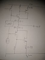
Those 0.1 Ohm resistors are a good idea which avoid depending on the functioning of a complicated temperature compensated amplified diode. In my design, if the amplified diode fails while the output is hot, it would mean destruction of the output transistors.
P.S.
Those 0.1 Ohm resistors are a good idea which avoid depending on the functioning of a complicated temperature compensated amplified diode. In my design, if the amplified diode fails while the output is hot, it would mean destruction of the output transistors.
Last edited:
Let evolution take its course. There is no hurry and no money to be lost.
P.S.
Those 0.1 Ohm resistors are a good idea which avoid depending on the functioning of a complicated temperature compensated amplified diode. In my design, if the amplified diode fails while the output is hot, it would mean destruction of the output transistors.
Exactly.
What I have shown is standard way to implement CFP OP stage.
The resistor values vary to some degree, but you need them.
T
To implement output short circuit protection and other protections, I am afraid I am faced with requiring a custom built opto-coupler. This requires three sensor LEDs and a high voltage transistor.
I don't know how many diyaudio users have made custom components, besides winding difficult to find transformers to power tube amplifiers, although a flyback switching power supplies can power a tube amplifier.
The idea behind the weird opto-coupler is to use one LED in series with the sensor transistor, so that once it is activated, it remains on by supplying current to the sustaining LED. The other two LEDs would activate the circuit by sensing overload currents from the +ve and -ve sides of the power stage.
P.S.:
Instead of trying to outsmart Einstein, something I am incapable of doing, is there an output overload protection circuit I can use without requiring specially made components? A circuit that brings the output to zero current would be ideal, but I am afraid that requires more complicated circuitry.
Last edited:
Its not easy is it ?
Short circuit protection and overload protection aren't quite the same. For overload protection you can sense the current and use that information to apply a mute to the amplifier input, either a hard mute or attenuation of some kind.
A short circuit means the feedback loop will lose control and that the output stage deliver massive current. Removing the input signal wouldn't reduce the output overload in this case... at least not unless there was sufficient resistance in the output circuit to allow the feedback to regain control.
Its difficult trying to re-invent what has been common practice for decades, and that is the standard output protection scheme that monitors current across a low value resistor in the output stage.
Rethinking again and reverting back to the idea of denying power to the amplifier, in the event of overload/shorted output, I think, it can be done with an additional six components. This time the opto-coupler is a normal one transistor one diode optocoupler. For low current sensitivity an infrared LED may be used provided these photons have enough energy to generate electron-hole pairs in a doped silicon crystal.
I am attaching the edited yet unsimulated circuit. First, I have to figure out how to let LTSpice recognize a tyristor. The problem is I do not know what I have to type in the Component Attribute Editor dialog. I need to simulate a 0.5A tyristor that can stay on with a few milliamps and can be triggered with a current in the order of a milliamp.
P.S.
With this optocoupler the LED conducts when the current reaches 13A.
Attachments
Last edited:
I've used a triac once in LT but I had to ask how to do it.
See if this works, it might give you (and me) some clues how I did it.
Edit... This must have been the thread where I asked:
Triacs in LTspice. Where can I get a model.
See if this works, it might give you (and me
) some clues how I did it.Edit... This must have been the thread where I asked:
Triacs in LTspice. Where can I get a model.
Attachments
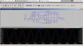
I will stick with the conventional output current limiting circuit. The attachment is the resultant circuit. with a short circuit of resistance 0.1 Ohms the output current is 28A and the output waveform is more or less a square wave.
If users think this circuit is the one to be built, I will start making the PCBs. Each amplifier circuit will consist of 3 separate PCBs two for the output stage and another one for the other stages.
If users think this circuit is the one to be built, I will start making the PCBs. Each amplifier circuit will consist of 3 separate PCBs two for the output stage and another one for the other stages.
Attachments
That looks workable. The addition of a resistor from the base of each limiter to the appropriate rail also allows changes in Vce of the output devices to figure into the equation. You can scale the resistors to allow full output into your chosen load impedance and yet greatly limit the current into a short circuit.
Not so sure on D5 and D6 tbh as you are relying on the caps to pull charge out of the base at high frequency. The base of the drivers are almost floating when reverse biased.
Not so sure on D5 and D6 tbh as you are relying on the caps to pull charge out of the base at high frequency. The base of the drivers are almost floating when reverse biased.
a) I also heeding to the advice of mounting the driver transistors on a separate heatsink. Simulations show that if the drivers' temperature is 10K cooler than the main heatsink, the quiescent currents will be optimum.
b) Ringing of the drivers' base current at 16kHz is eliminated with compensating signal diodes and a 3n3 capacitor in parallel.
It seems, this is it! Now, the dirty work of PCB making... dirty, but exciting...
b) Ringing of the drivers' base current at 16kHz is eliminated with compensating signal diodes and a 3n3 capacitor in parallel.
It seems, this is it! Now, the dirty work of PCB making... dirty, but exciting...
Thanks for this. I added a 6k8 resistor in parallel with the Base-Emitter junctions of the drivers. The bias was also accordingly modified. The modified circuit is attached.Not so sure on D5 and D6 tbh as you are relying on the caps to pull charge out of the base at high frequency. The base of the drivers are almost floating when reverse biased.
P.S. I think, an aggressive calculation intensive simulation is a good thing to do at this point. So, I will try to force LTSpice to use maximum accuracy and limit the time step maximum down to 10pSec.
Attachments
Last edited:
Thanks for this. I added a 6k8 resistor in parallel with the Base-Emitter junctions of the drivers. The bias was also accordingly modified. The modified circuit is attached.
P.S. I think, an aggressive calculation intensive simulation is a good thing to do at this point. So, I will try to force LTSpice to use maximum accuracy and limit the time step maximum down to 10pSec.
So what happens if a voltage spike is generated across the output transistors when an attempted termination of output current occurs at high power outputs?
- Home
- Amplifiers
- Solid State
- My attempts at a design of a 3 stage amplifier