Yes there is a mistake in my calculation of the closed loop gain I should not have included R31 in this. Leaving this aside the theoretical closed loop gain is the value of R5/R10 +1.
This is reduced by roughly 12% of the input voltage due to the divider action of R1 and the parallel combination of R23 and R12. There is no attenuation of the input of the original circuit so yours has more closed loop gain than it might appear from your testing. That becomes important for the inverting input of your amplifier where yours has the greater amount. You can work these theoretical figures out for yourself.
With regard to the LTP your BC337-40 transistors used for Q5 and Q6 should be blameless.
I looked at these in a 1kHz sine wave simulation to study the impact of R31 on the operation since this configuration departs from normal practice where the results for both transistors should look alike. The tail current plot also does not resemble a sine wave as it should.
On the question of using the op.amp it appears this is further away from the transformer than the power amp boards and being small it should be relatively easy and make sense to shield this and use the gain of two to reduce the closed loop gain of the power amp boards which are more at risk due to proximity with the transformer.
Attachments
The last paragraph of the previous post is a drastic solution which I want to avoid as it renders all my past efforts useless.
Back to the Current Amplifier Implementation:
Recalling the testing to discover what is generating the hum issue, I remember, I unbolted the large toroidal transformer and placed it out of the metal amplifier box. The wires connecting the transformer permitted it to stay just out of the box, but resting on a side inclined facing out of the box. Testing for the persistent hum, there was no difference. This should mean, the cause of the hum is not the proximity of the transformer to the amplifier's sensitive circuitry, but something more subtle. I remember also connecting filtering capacitors to the current sources' bias, which are still soldered, and to the cascodes' bias. In all these, there was no change in hum.
So, according to logic, the cause of the hum must be something I did not test for, and something that has a strong bearing on the amplifier's ability to reject the power supply's imperfections. This something should be the differential pair, as those two are responsible for power supply rejection.
The problem with using a two resistor potential divider is the fact, that the cascode's bias voltage would be directly dependent on the instantaneous power supply voltage. This implies it would also be dependent on the ripple.
Searching online I confirmed that Zener diodes are actually used as noise generators, and that their noise generation, is large when lower currents flow. This is my case: I am using the Zener with a fraction of its current rating; this means, it is behaving like a noisy component. This may explain the random bursts of oscillations I got when I measured the noise at the output with an oscilloscope.
I have seen using a chain of series connected signal diodes instead of Zeners. Is a chain of forward biased signal diodes quieter compared to a Zener diode?
The three graphs for the input tail current become accurate sine waves when the three diode chain of the VAS is disconnected. Since, these three diodes are forcing the differential pair to depart from conducting a sinusoidal current when a sinusoidal signal is applied, it seems the source of trouble may be linked to them.
Thank you so much for this valueable diagnoses.
I'm sure I mentioned this earlier but have you tried adding a dummy load across each rail at the reservoir cap to increase ripple? Use a suitable bulb such as a 500 watt halogen. Try each rail in turn and see if the level of hum alters. That might give a clue as to the route of injection in the case of it being rail and layout related.
The three graphs for the input tail current become accurate sine waves when the three diode chain of the VAS is disconnected. Since, these three diodes are forcing the differential pair to depart from conducting a sinusoidal current when a sinusoidal signal is applied, it seems the source of trouble may be linked to them.
Thank you so much for this valueable diagnoses.
A while ago you posted a version of your circuit with 40 volt supply rails. I assume this was with light bulb in the transformer primary.
You have since reported a peak voltage in excess of that which prompts the question what is the normal voltage on the supply rails.
The higher this is the more concern there will be about your short circuit protection settings to ensure the safe operating area of the combined output transistors is not exceeded.
The Wharfedale technical manual shows the protection circuit for this is more complex. It would need to be in order to output 620 W into 2R loads. That might be necessary for professional use - do you really need that much at home.
These are the changes to the circuit implemented:
This amplifier will not be used for professional purposes but only at home. As rightly asked by mjona, at home these kind of powers are unnecessary. Therefore, I am opting to use the amplifier with a 42V DC per rail. I am achieving this by first stepping down the mains supply voltage, 230V, 50Hz, to 120V AC.
Carefully listening into the speakers after the changes listed above have been implemented, it is clear the random noise has been reduced and also the ripple. In one channel, this is just above barely audible. This channel is the farthest from the toroidal transformer. This channel also exhibits some degree, although greatly reduced, of crackling noise. I am associating this with the large, 2200uF, electrolytic at the inverting input.
Since copper strip is not easily accessible, I am thinking about using aluminium instead. The resistivity for aluminium is 2.82x10^-8 Ω·m. That for copper is 1.68 Ω·m. This means a thicker layer is necessary to produce the same effect as copper.
The output short circuit current can be restored to symmetry by adding a BC807 transistor and a signal diode to replace the VAS's three signal diode chain. This addition does not cause the differential pair currents to depart from a sine wave.
Only true with 8 Ohms output.
If instead of a signal diode, two resistors are used, the differential pair currents remain sinusoidal down to a load impedance of 4 Ohms.
The circuit is attached.
P.S.
As short circuiting the output is a serious mistake often with expensive consequences, I always make sure the outputs are properly connected before powering such powerful equipment.
The two MJE15033 and MJE15032 driver transistors have differing amplification factor (beta) with one almost twice the other. This puts unnecessary stress on the input stage to deliver symmetrical sine waves for both half cycles.
- The cascodes's bias Zener diode has been replaced with a 2k resistor in parallel with a 47uF electrolytic capacitor.
- A 10 Ohm resistor has been inserted to split the signal ground from the power ground.
- The VAS's three series signal diodes chain has been removed.
- The 2.4k resistor in series with the base of the inverting input has been removed.
- The two series signal diodes used as a bias for the current sources for the VAS and input stage now are in parallel with a 33uF electrolytic capacitor and a 100nF polyester capacitor.
This amplifier will not be used for professional purposes but only at home. As rightly asked by mjona, at home these kind of powers are unnecessary. Therefore, I am opting to use the amplifier with a 42V DC per rail. I am achieving this by first stepping down the mains supply voltage, 230V, 50Hz, to 120V AC.
Carefully listening into the speakers after the changes listed above have been implemented, it is clear the random noise has been reduced and also the ripple. In one channel, this is just above barely audible. This channel is the farthest from the toroidal transformer. This channel also exhibits some degree, although greatly reduced, of crackling noise. I am associating this with the large, 2200uF, electrolytic at the inverting input.
Since copper strip is not easily accessible, I am thinking about using aluminium instead. The resistivity for aluminium is 2.82x10^-8 Ω·m. That for copper is 1.68 Ω·m. This means a thicker layer is necessary to produce the same effect as copper.
The output short circuit current can be restored to symmetry by adding a BC807 transistor and a signal diode to replace the VAS's three signal diode chain. This addition does not cause the differential pair currents to depart from a sine wave.
Only true with 8 Ohms output.
If instead of a signal diode, two resistors are used, the differential pair currents remain sinusoidal down to a load impedance of 4 Ohms.
The circuit is attached.
P.S.
As short circuiting the output is a serious mistake often with expensive consequences, I always make sure the outputs are properly connected before powering such powerful equipment.
The two MJE15033 and MJE15032 driver transistors have differing amplification factor (beta) with one almost twice the other. This puts unnecessary stress on the input stage to deliver symmetrical sine waves for both half cycles.
Attachments
But most of the time the input stage is mainly driving the VAS compensation capacitor, whose current requirements are not dependent on the drivers' current gain. The VAS transistor has provide the current for the driver, not the input stage. Only at the low frequencies is the input stage seeing the driver load directly, and then there is an abundance of open-loop gain to linearize the amp.
Studying the short circuit protection for this circuit, one should immediately realise, the circuit starts shunting the drivers' base currents when the latter exceed the maximum base current at maximum load and current output. Such a protection circuit will therefore allow a short circuit current that is beyond the normal maximum output current, and the output transistors will be burdened with the full supply voltage. This means, they will not be working within the safe operating area.
An 'intelligent' short circuit protection, would constantly analyse the output changing state whenever an output current overload is sensed. This would trigger other circuitry to deny the output of driver current. However, a circuit like that, would require some state remembering circuitry, which often translates to some form of logic.
The output short circuit protection circuitry has been recommended to me by well respected members of these fora. The basis for their recommendation was, that this protection circuit, has been in use for many years and it provides sufficient protection for many users.
An overhaul of the protection circuitry, would require a redesign of the entire amplifier module that includes all signal handling before the driver stage. Since what I implemented as a protection circuit was suggested by very respectable forum members, I am sticking to it.
If your mains voltage is 240 volts ac by what means are you reducing that to 120 volts ac.This amplifier will not be used for professional purposes but only at home. As rightly asked by mjona, at home these kind of powers are unnecessary. Therefore, I am opting to use the amplifier with a 42V DC per rail. I am achieving this by first stepping down the mains supply voltage, 230V, 50Hz, to 120V AC.
Carefully listening into the speakers after the changes listed above have been implemented, it is clear the random noise has been reduced and also the ripple. In one channel, this is just above barely audible. This channel is the farthest from the toroidal transformer. This channel also exhibits some degree, although greatly reduced, of crackling noise. I am associating this with the large, 2200uF, electrolytic at the inverting input.
Since copper strip is not easily accessible, I am thinking about using aluminium instead. The resistivity for aluminium is 2.82x10^-8 Ω·m. That for copper is 1.68 Ω·m. This means a thicker layer is necessary to produce the same effect as copper.
The output short circuit current can be restored to symmetry by adding a BC807 transistor and a signal diode to replace the VAS's three signal diode chain. This addition does not cause the differential pair currents to depart from a sine wave.
P.S.
As short circuiting the output is a serious mistake often with expensive consequences, I always make sure the outputs are properly connected before powering such powerful equipment.
If that is going to be a voltage step down transformer you should be thinking about replacing the one in the equipment. That will give you the chance to include a screen between the primary and secondary winding which could reduce noise getting into your system - like the suspect crackling you are hearing. You could also specify a copper strap around the outside of this. You could possibly get away with a 300VA rated toroid which should be more compact and have a lower stray field.
With 42 volt supplies you could dispense with the load line limiting transistors for the output stage and substitute rail fuses. The safe operating area of 4 pairs of output transistors should be enough to withstand a short before the rail fuses blow. Your protection for the Vas transistor can be beefed up by direct connection of the BC807 minus the added biasing. If you absolutely need these extra resistors then something else in your circuit needs to be changed.
Calculation for power dissipation when the output is short-circuited.
Assuming a maximum power of 650W into 2 Ohms:
P = I^2*R/2 (calculating for a pure sine signal)
==> 650 = I^2*2/2
==> I = sqrt(650)
==> I = 25.5A peak
Let us assume short circuit protection limits the short circuit output current to 27A.
Simulations show this current is a square wave implying the equivalence of DC:
Therefore, the power dissipation on short circuit of the output would be:
P = IV (DC power output)
==> P = 27*80
==> P = 2160W
This power is shared between 16 power transistors, therefore the dissipation per transistor would be:
power/transistor = 2160/16 = 135W
The thermal power rating of 2SA1943 and 2SC5200 is 150W. The result is within limits.
Proposed Solution:
This should be such as to limit the output current to 27A on short circuit. Lowering the VAS's standing current did not have any effect.
Last edited:
Proposed Solution:
The solution was to change the base resistors of the short circuit protection circuit to 2.2kOhm. Now, the short circuit current is 25A peak. This is within the tolerable limit for the output devices.
With this change, while delivering 620W average power into a 2 Ohm load, the distortion figure is slightly higher at 0.055%. With an 8 Ohm load, the distortion is at 0.016% and with a 4 Ohm load, it is 0.011%.
Note:
I am very thankful for the protection circuit given as it is simple and effective. My modifications, improved on the original circuit design by reducing the distortion figure from 0.5% to these nice figures.
Due to the many circuit changes the PCB is a little battered. However, with patience and careful mechanical modification planning, this battering was greatly minimised. In the end, when I am satisfied with the outcome, a little surgical spirit and some more patience to clean the PCBs, will put this project to a hopefully a long life of accurate sound amplification.
Again, special thanks go to mooly, the nice moderator, mjona and all the others who made this learning journey possible.
Before joining this forum, I did not realise that electronic component parasitics were more often than not significant, and I have been practicing electronics since I was a late adolescent.
")
Calculation for power dissipation when the output is short-circuited.
Assuming a maximum power of 650W into 2 Ohms:
P = I^2*R/2 (calculating for a pure sine signal)
==> 650 = I^2*2/2
==> I = sqrt(650)
==> I = 25.5A peak
Let us assume short circuit protection limits the short circuit output current to 27A.
Simulations show this current is a square wave implying the equivalence of DC:
Therefore, the power dissipation on short circuit of the output would be:
P = IV (DC power output)
==> P = 27*80
==> P = 2160W
This power is shared between 16 power transistors, therefore the dissipation per transistor would be:
power/transistor = 2160/16 = 135W
The thermal power rating of 2SA1943 and 2SC5200 is 150W. The result is within limits.
Proposed Solution:
This should be such as to limit the output current to 27A on short circuit. Lowering the VAS's standing current did not have any effect.
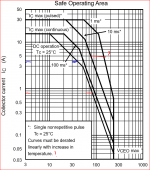
Don't rely on that. The graph for the safe operating area of a 2SC5200 attached shows that with 42 volt rails your IC can be close to 4A per each. With 80 volt rails you are down to 800 m.A. which implies to deliver peak currents exceeding this amount one is relying on a delayed action protection sufficient to allow these to pass before the limiter prevents the output stage from getting outside the safe operating area.
You should run a DC op pnt simulation to ensure the safe limits are not exceeded with various test loads including a short. Check the currents across the 0.1R resistors are not passing damaging levels of current - possible if the output halves have differing bias currents in their respective chains.
Attachments
I made a mistake. Calculations require a crisp mind fully aware of all details, and due to my not so youthful age, I forgot.
Each amplifier channel has 8 power transistors, not 16. So, the estimated thermal power dissipated per device is twice what I calculated. This is far outside the safe operating area.
Recalculating for a 25A peak current when the short circuit protection is active, the thermal dissipation per output device is, V*I = 25*77 = 1925W. For eight output devices, this is: 1925/8 = 240.6W.
At this point, the crucial question is, whether the actual short circuit current limiter provides protection for the output devices, and for how long? If we are beyond the manufacturer's thermal dissipation maxima, it means, the output devices' thermal channels cannot efficiently transfer that thermal energy quickly enough to deter temperature from rising catastrophically. This is my reasoning, but sometimes, even apparently very logical reasoning may not mirror what reality may have in store.
Speculating about using a Schmitt Trigger:
An interesting circuit is some kind of modified Schmitt Trigger that stays off when the maximum current is not exceeded by a certain allowable margin, and when this limit is reached, it turns itself into a low resistance path until the voltage across it drops well below the triggerable voltage.
Taking the graph from #532, and lets suppose +/-50V rails.
An output short to ground would mean the output device sees 50V, which has a max current of 3A for continuous operation. Thus the limit would need to be 3A per device.
But if opposite output devices failed shorted, then the voltage would be 100V, meaning about 0.45A max would be allowed. With a 3A limit the device is toast - ie the initial device failures cascade across to the others, taking out the whole output section.
Assuming a single pair of output transistors. A 30V peak output signal into 4 ohms would require 7.5A peak (when the output device sees 50-30 = 20V), which is just on the limit.
A 40V peak output into 4 ohms requires 10A peak (10V across the output device), again OK.
Basically a single pair of output devices can just handle 4 ohms resistive at any amplitude, but the 3A limiter would cut in at 12V peak signal. Not great.
The realization is that anVI limiter is much much preferred, in fact a dual slope VI limiter circuit does even better, conforming to the device limit curve more closely and getting more from the output devices without compromising overload prevention. It could both prevent the cascade failure when one output device goes shorted, yet allow 10A or more at the peaks of a 4 ohm waveform.
Thought of another way it allows fewer output devices by protecting them more accurately.
Last edited:
Thank you so much.
I was taking the safe operating power of power transistors too simply. Since thermal runaway is very real, Vce is a dominant limiter, as more voltage mean, a stronger electric field across the junctions, which pulls off more electrons across them. There is also the limitation of impurity non-uniformity of the transistor silicon die itself. The latter imperfection, gives rise to localised high current paths that generate too much heat per unit volume with the consequence of localised silicon die damage.
I was taking the safe operating power of power transistors too simply. Since thermal runaway is very real, Vce is a dominant limiter, as more voltage mean, a stronger electric field across the junctions, which pulls off more electrons across them. There is also the limitation of impurity non-uniformity of the transistor silicon die itself. The latter imperfection, gives rise to localised high current paths that generate too much heat per unit volume with the consequence of localised silicon die damage.
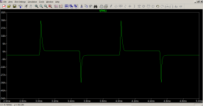
With the addition of two transistors, the change of two resistors, and the addition of another two resistors, the output overcurrent protection circuit is now greatly reducing the short circuit power dissipation in the output transistors. However, the current waveform is slightly not symmetrical about the time axis (X-axis).
Attachments
One final thing you need to do which I believe I mentioned before is to fit reverse connected rectifier diodes in parallel with the output transistors in each rail.
The reason for this if the protection circuit works at high output power the speaker load will generate emf - a current which has nowhere to go will result in a reduction of current and a spike in voltage - a change in the shape of the energy envelope.
If you look at the original circuit for the Wharfedale MP1200 or any similar high power amplifier circuit you will see these in place. The purpose of these is to divert spikes away from the power devices whose VCEO ratings will otherwise be at risk of failure.
You need to have these as an insurance policy. It would be best to make these rectifiers high current and high switching speed types.
Those diodes are installed.mjona said:One final thing you need to do which I believe I mentioned before is to fit reverse connected rectifier diodes in parallel with the output transistors in each rail.
The secondary breakdown is due to the positive tempco of current flow at a given Vbe - the hotter areas have more current flow and thus get even hotter, no non-uniformity is needed initially, just random fluctuations which are always present, but of course real devices will have some non-uniformity.Thank you so much.
I was taking the safe operating power of power transistors too simply. Since thermal runaway is very real, Vce is a dominant limiter, as more voltage mean, a stronger electric field across the junctions, which pulls off more electrons across them. There is also the limitation of impurity non-uniformity of the transistor silicon die itself. The latter imperfection, gives rise to localised high current paths that generate too much heat per unit volume with the consequence of localised silicon die damage.
Secondary breakdown is more of a problem with large power devices where the die is larger, allowing temperature differences to build up. Its the main reason output devices are paralleled, rather than using really big transistors. Emitter resistors allow fair current sharing between devices and prevents secondary breakdown between devices (where the hotest device hogs most of the current).
- Home
- Amplifiers
- Solid State
- My attempts at a design of a 3 stage amplifier