That would be exultant for me, but understanding down to minute details is very very time consuming. I am a person, who due to wanting to understand down to details, takes far longer than others to understand.Oh, no, man, it couldn’t be just added... You must understand precise balance of this system, gain margin and phase margin, influence to the overshoot and rise speed...
My knowledge of electronics still lacks the quantitative aspect of filters and, it seems, amplifier stages. The latter, due to their intrinsic capacitance influence phase and gain as frequency is changed. However, the mathematics is extremely cumbersome if one goes the 'from basic principles' route. A simple RC filter becomes a daunting complex number calculation as I will briefly illustrate:
Let us assume we have an RC network fed by V at f Hertz.
The impedance of the whole network is:
Z = R + Xc
Let us assume we are measuring the filtered signal across C.
So, the quotient Q = Xc/(R + Xc)
Let us now introduce complex numbers in the expression:
Using p to stand for pi = 3.142 approx
Q = [ -j/(2pfC) ] / [ R - j/(2pfC) ]
To get rid of the imaginary part in the denominator, multiply both numerator and denominator by the complex conjugate of the denominator.
Q = { [ j/(2pfC) ]*[ R + j/(2pfC) ] / [ R^2 + 1/ ((2pfC)^2) ]
For clarity let us represent the denominator by D.
So, Q = (1/D)*[ jR/(2pfC) - 1/((2pfC)^2) ]
Most circuits require more complex LCR networks giving rise to longer and more complex formulae.
The required calculation complexity is what is keeping me back from developing the skills necessary for successful circuit design.
P.S.
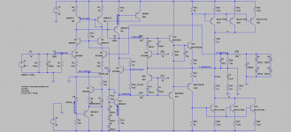
I installed LTSpice on my Windows partition but I need to ask how I can make spice recognize schematics made with KiCad?
Thanks for everyone's patience.
The rapidly increasing complexity of the math is exactly why we use simulation.
There may be a way to export a net list from KiCAD that’s useable in LTspice, but I generally just draw the schematic twice. The spice version can be simplified some, omitting filter caps and such forth.
There may be a way to export a net list from KiCAD that’s useable in LTspice, but I generally just draw the schematic twice. The spice version can be simplified some, omitting filter caps and such forth.
Don't waste your time...I installed LTSpice on my Windows partition but I need to ask how I can make spice recognize schematics made with KiCad?
P.S.
I installed LTSpice on my Windows partition but I need to ask how I can make spice recognize schematics made with KiCad?
Thanks for everyone's patience.
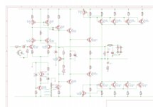
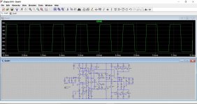
Here is the simulation file in case you want to have a play. I changed a few things to get a reasonable performance as there were severe performance limitations when squarewave testing.
You will need to rename the text file of models and add it to the simulation in place of the one I used.
Good luck
")
Attachments
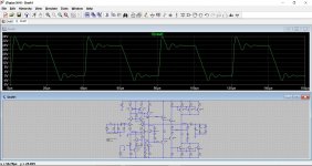
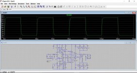
Finally, I got the square wave plot.
From the previous simulation, we found that the frequency response extends well into ultrasonic frequencies to several hundred kilohertz. The square wave distortion suggests some harmonics were not amplified, or better, that the bandwidth is not wide enough. For an audio amplifier this cannot be what is causing the distortion of the square wave. I think, it is a poor dV/dt, slew rate. So, I must redesign the VAS with aim of improving the slew rate. The Miller Capacitance is too low to be the cause. I am tempted to think, the MJE340 and MJE350 are the cause. Hm, if I use a cascode to prevent both Base-Collector junction capacitances from experiencing voltage changes, I might get a better dV/dt (slew rate).
One itching question is: is a square waveform with T = 40 micro-seconds of the right frequency? Such a period belongs to a frequency of 25kHz. So, with 'our' huge bandwidth, that should be space enough for up to the 16th harmonic (assuming a bandwidth of 400kHz). Sixteen harmonics give rise to a better approximation for the square wave. So, I conclude it must be the slew rate that is degrading performance.
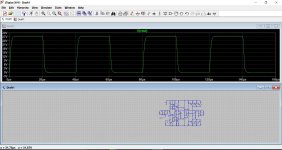
The sim file I attached has the front MJE devices replaced with smaller and faster ones.
As well as looking at the output voltage, also look at the input voltage across the filter. That has the (wanted) effect of reducing slew rate. I also added a small cap across the feedback resistor to introduce a small amount of phase lead compensation.
If we go all out and remove the above caps we appear to get a better square wave response but I would caution against trying to squeeze the last bit of rise time this way as it will be at the expense of stability.
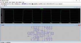
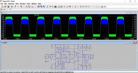
So here is the slew rate under these conditions. I've also added an 8 ohm resistive load.
So over 1uS the amp slews at approximately 22v/us which is pretty decent in practice.
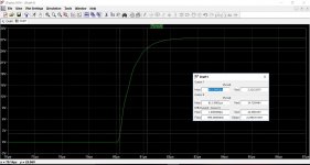
The last image is with the input filter cap back in place and looking at the voltage across this cap (the input to the amplifier.
As well as looking at the output voltage, also look at the input voltage across the filter. That has the (wanted) effect of reducing slew rate. I also added a small cap across the feedback resistor to introduce a small amount of phase lead compensation.
If we go all out and remove the above caps we appear to get a better square wave response but I would caution against trying to squeeze the last bit of rise time this way as it will be at the expense of stability.
So here is the slew rate under these conditions. I've also added an 8 ohm resistive load.
So over 1uS the amp slews at approximately 22v/us which is pretty decent in practice.
The last image is with the input filter cap back in place and looking at the voltage across this cap (the input to the amplifier.
Attachments
Thanks for helping me. I am excited seeing my amplifier circuit evolving.
Till now, there is no overload current protection. I am adding two transistors to divert the driver current away from the output transistor's bases. I have seen this circuit online. Adding a light emitting diode indicator would inform users that their amplifier is reaching overload point.
Another idea is to use an automatic gain reducer when the output nears maximum preventing overload.
I think, it may be done using an opto-coupler. The diode sensor section would be connected across one 0.22 Ohm, those found on the emitters of the output transistors, while the output transistor would shunt the biasing input resistor at the base of the differential pair.
Additionally, a clip detector is also to be added. Mathematically, a clip is when dV/dt = 0 and stays like for a period instead of assuming zero value instantaneously. A small capacitor feeking the base of a transistor is sensitive to dV/dt since Q = CV and hence, dQ = CdV which leads to dQ/dt = C*dV/dt. The latter is what we want. This means, the output of a transistor connected in that way goes high when the output clips. To sense non-zero durations a capacitor connected across the output resistor, would allow the output to rise with a delay. This arrangement, should also sense clips that do not take place at the outputs maximum. Such clips are also fatal for loadspeaker coils as there is no reactive components at clips irrespective of whether they take place at maximum output voltage or not.
The easiest way to add current limiting would be to include a low value resistor in the collector path of the output devices and sense volt drop across those. Using an opto and sensing across the 0.22 ohm is possible but would add to the complexity. An LED in an optocoupler needs around 1.7 volts before it will conduct. That implies a current of around 7 amps, and you have three pairs... you could add sophisticated electronics to derive an LED control voltage that was referenced to each rail (as the 0.22 ohms are) but the circuitry would be as complex as the main amp.
Detecting clipping can be done with an opamp monitoring the voltage difference between the - and + inputs of the amplifier. When clipping occurs the amp losses control and a big voltage difference will occur between the two inputs. An opamp can detect that and light an LED but you need extra circuitry to make the LED light for a reasonable time. Clipping for 1ms would be barely visible from the LED, so you need a pulse stretcher such as a monostable to light the LED for say 2 seconds each time a clip event is detected.
Detecting clipping can be done with an opamp monitoring the voltage difference between the - and + inputs of the amplifier. When clipping occurs the amp losses control and a big voltage difference will occur between the two inputs. An opamp can detect that and light an LED but you need extra circuitry to make the LED light for a reasonable time. Clipping for 1ms would be barely visible from the LED, so you need a pulse stretcher such as a monostable to light the LED for say 2 seconds each time a clip event is detected.
I hopefully implemented output current limiting with two transistors which divert current away from the output transistors' bases as drive current increases.
For clipping prevention, the output can be rectified and the resulting unidirectional signal used to light a LED when a threshold voltage is reached.
P.S.
Does this site support png images?
For clipping prevention, the output can be rectified and the resulting unidirectional signal used to light a LED when a threshold voltage is reached.
P.S.
Does this site support png images?
Attachments
png is fine
In your arrangement the limiter transistor will pass a massive current when it is activated.
Have a look at this which acts on the pre driver transistors. The VAS stage also has a limiter added which is essential to prevent this stage trying to supply lots of current when the protection activates. Not only can the current limit be more precisely defined, it can also be modified by adding a divider network to the protection transistor bases. You could also go further and partially bias these transistors by a resistor to each supply. That allows for the circuit to more closely follow a safe operating curve SOAR) whereby the protection also follows the supply voltage. If the rails are raised the limiting occurs at a lower current.
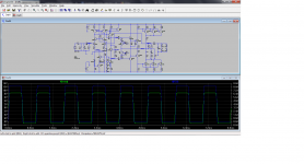
This shows what happens when a 1 ohm load is applied at full output. The voltage swing is limited (in green) and the output transistor current for one of the devices is shown (in blue).
In your arrangement the limiter transistor will pass a massive current when it is activated.
Have a look at this which acts on the pre driver transistors. The VAS stage also has a limiter added which is essential to prevent this stage trying to supply lots of current when the protection activates. Not only can the current limit be more precisely defined, it can also be modified by adding a divider network to the protection transistor bases. You could also go further and partially bias these transistors by a resistor to each supply. That allows for the circuit to more closely follow a safe operating curve SOAR) whereby the protection also follows the supply voltage. If the rails are raised the limiting occurs at a lower current.
This shows what happens when a 1 ohm load is applied at full output. The voltage swing is limited (in green) and the output transistor current for one of the devices is shown (in blue).
Attachments
KiCad
I also am a KiCad proponent, having used it for a number of years for both personal and commercial projects. I agree that it has some quirks, as do all of the similar programs. It has always produced reliable Gerber plots to send to the board vendor. I can't say the same for at least one of the major paid for tools that starts with an A.
I also am a KiCad proponent, having used it for a number of years for both personal and commercial projects. I agree that it has some quirks, as do all of the similar programs. It has always produced reliable Gerber plots to send to the board vendor. I can't say the same for at least one of the major paid for tools that starts with an A.
Thanks for everyone's little and not-so-little help in this thread. I think, the crossover distortion limiting bias has to be redesigned. Effectively, there are four base-emitter junctions in parallel with the amplified diode. This means, for current to start flowing through all four bases, a voltage between 0.5x4 = 2V and 0.7x4 = 2.8V, is required. Since, the current in the primary stage of the VAS is very low, the resistors for the amplified diode are large. To lower these resistors a larger VAS current is required.
I will use a constant current of 2.5mA and allow an amplified diode resistance chain current of 15% of 2.5mA = 375μA.
For a voltage of 0.7x2 + 1.2 = 2.6V, the resistance is: 6933 Ohms or 7kOhms.
The resistor value across the base-collector junction is:
(2.6 - 0.7)/375E-6 = 5067 Ohms ( i.e. 5kOhm)
The resistor across the emitter-base junction is: 0.7/375E-6 = 1867 Ohms ( i.e. 1.9kOhm)
The resistance across the emitter-base must include a variable resistor for fine control of the total voltage. Let us assume a 470 Ohm is used with a remaining series resistance of 1600 Ohms.
With preset set to zero we get a voltage of:
0.7*(5000 + 1600 + 0)/(1600 + 0) = 2.89V
With the preset set to 200 Ohms:
0.7*(5000 + 1600 + 470)/(1600 + 470) = 2.39V
I had to fiddle with numbers until I found this voltage range which includes the 2.6V value.
Now, let us recalculate the resistor chain current:
At 2.89V:
2.89/(5000 + 1600) = 438μA
At 2.39V
2.39/(5000 + 1600 + 470) = 338μA
For primary stage of the VAS:
The current sources emitter resistance will be:
(3*0.7 - 0.7)/2.5E-3 = 560 Ohms
Since the output of the current mirror automatically adjusts its output voltage, I think, although I may be wrong, there is no need to change the emitter resistance of the VAS's amplifying transistor.
These are my humble calculations.
These were the values I ended up with. VAS current is approximately 6ma which is a fairly typical value. If you go to low then you may struggle to get good HF performance as well as running into problems of lack of driver current under extreme loading.
Set your own goals and specifications (such as gain, frequency response, slew rate and the currents you wish the output stage to limit at) and then change the design to meet your targets.
Set your own goals and specifications (such as gain, frequency response, slew rate and the currents you wish the output stage to limit at) and then change the design to meet your targets.
Attachments
Here's Michael Kiwanuka's comments in his VI limiting article on the location of this capacitor. "A small-value capacitor is sometimes connected across the base-collector junction of each protectionMooly!
Just add 330p-1n B-C capacitors to the protection transistors. This will avoid the oscillation during limiting.
Sajti
transistor1 with a view to eliminating oscillation that occurs in the network during the limiting
process. These capacitors appear in parallel at AC and are entirely unsatisfactory, as they create an
ill-defined and therefore undesirable feedfoward path around the output stage, shunting it out of the
global feedback loop at high audio frequencies-precisely where the amplifier is most vulnerable with
respect to non-linearity.
Such vulnerability is due to a necessarily diminished feedback factor at high audio frequencies in the
interest of Nyquist stability. Connecting the capacitor across the base-emitter junction of each
protection transistor is the preferred solution."
Brian
Sorry, I mistakenly mentioned the VAS but that current is suitable for the differential pair. In fact, the latter is calculated to have a constant current of 3mA. The VAS's constant current is around 9mA and the next stage is a buffer.
Now, I will silence myself and try to make use of LTSpice. Till now, I am unsuccessful of simulating my edited schematics. At this moment, eschema is complaining that I have missing connections when I run the rules test. The precise text of the error is:
"Pin not connected and no connect symbol found on this pin." It shows a green arrow and that is it.
I did not connect anything to the input and did not connect a power supply to the power tracks. I have no idea how this is done. I want to simulate my circuit with a power supply voltage of -85V, 0V, +85V. At maximum load this will have a severe ripple: I calculated about 13.3V peak to peak. The power supply uses 6600 Micro-Farads on each rail and the rectifier bridges are of the square metal case type.
Here's Michael Kiwanuka's comments in his VI limiting article on the location of this capacitor. "A small-value capacitor is sometimes connected across the base-collector junction of each protection
transistor1 with a view to eliminating oscillation that occurs in the network during the limiting
process. These capacitors appear in parallel at AC and are entirely unsatisfactory, as they create an
ill-defined and therefore undesirable feedfoward path around the output stage, shunting it out of the
global feedback loop at high audio frequencies-precisely where the amplifier is most vulnerable with
respect to non-linearity.
Such vulnerability is due to a necessarily diminished feedback factor at high audio frequencies in the
interest of Nyquist stability. Connecting the capacitor across the base-emitter junction of each
protection transistor is the preferred solution."
Brian
Check out how much current runnnig from the VAS to the output through that capacitor! Very few uA. And you can reduce it further, applying some 10-12V Uce voltage across the protecting transistor.
Sajti
- Home
- Amplifiers
- Solid State
- My attempts at a design of a 3 stage amplifier