Using voltage/current limited supplies is a good plan and is something I do myself.
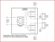
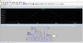
Solid state relays for speakers are becoming popular. They consist two suitable power FET's connected back to back. FET's with an Rds as low as a few milliohms are common these days. The gates are driven from a floating voltage source, typically a photovoltaic coupler. Very simple and very reliable.
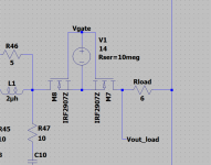
The LT image shows how to set up a simulation. V1 is the floating voltage source, >7 volts is on and 0V is off.
Solid state relays for speakers are becoming popular. They consist two suitable power FET's connected back to back. FET's with an Rds as low as a few milliohms are common these days. The gates are driven from a floating voltage source, typically a photovoltaic coupler. Very simple and very reliable.
The LT image shows how to set up a simulation. V1 is the floating voltage source, >7 volts is on and 0V is off.
Attachments
If you are looking for inspiration with electronic relays the attached link may be of interest.
TGM10 - based on NAIM by Julian Vereker
TGM10 - based on NAIM by Julian Vereker
The physical modifications of one channel are ready with the next phase being testing for current leaks. Low voltage testing at +/-15V, total 30V DC, is OK. The circuit is the modified output with large smoothing capacitors, 6600uF per supply rail. Since PCB cutting may short previously existing tracks, I am convinced making sure there are no short circuited tracks is extremely important at this stage. Therefore, I will use two mains 25W filament bulbs connected in series with the amplifier's power supply, with a bulb per rail, and see what happens. The modified circuit must pass these tests before the current limiting bulbs will be removed.
When this test is passed, the next phase will be of building a small PCB to host the VBE multiplier and variable resitors. The VBE transistor will be mounted physically on top of one of the 2SC5200/2SA1943 power transistors to sense the temperature of the power stage. This will ensure the bias voltage drops as power stage's temperature rises.
The succeeding testing will involve setting the proper VBE multiplier bias voltage. I will use two resistors instead of the VAS's driver and current source. The resistor values will be such that the VAS's standing current flows in the resistor, VBE multiplier, resistor chain. Again, the first step in the test will involve using protective mains filament bulbs. When this test is satisfied, I will use the full voltage without protection and test for stability over a period of time.
Readers may think this is unnecessary, but high voltage has no mercy on parts, which are costly to replace and take time to arrive by post.
There is not enough space for a separate PCB hosting the VBE multiplier. This means, I will make the final PCB that hosts the input stage, voltage amplifier stage, VBE multiplier and output current overload limiter. The latter two circuits will be assembled first to allow me to set the proper bias voltage with a collector current of 10mA per output transistor. As posted before I will test for stability with this quiescent current, then it will be time to assemble the input stage and VAS. The latter two stages will be tested before connected them to the output stage. I will take the negetive feedback from the collector of the VAS constant current source. This will allow me to first ensure the output voltage is kept at 0V with no signal. After this test, a signal will be connected and the AC signal strength measured at VAS's current source's collector.
The next step is connecting the VAS to the VBE multiplier, and moving the negative feedback point from the VAS's current source's collector to the output point. The next test will again limit the current with light bulbs to prevent damage to the output stage in the event high frequency oscillations occur. A frequency counter will be connected to the output to make sure there are no high frequency oscillations.
Next, it will be time for a proper power test with high power resistors across the output.
This is becoming interesting... it is a pity I am not doing it for a course of study.
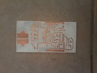
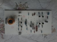
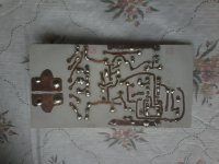
The preparation and etching of the PCB to host the input stage, VAS, VBE multiplier and output current limiter is etched and ready. I used an old 'fusty, musty, dusty' method and drilled all the holes before I completed the tracks. Thanks to the poster who suggested this simple yet extremely helpful tip.
My etch resist was not some difficult to get chemical, but correcting fluid from a local stationer. The correcting fluid remained solid through the entire etching process.
The next thing to do is to check for shorts. I can also reuse some components from the original circuit. There is a 50 Ohm ten turn preset and a 470 Ohm variable resistor that I can use. I can also use resistors, diodes and capacitors.
")
My etch resist was not some difficult to get chemical, but correcting fluid from a local stationer. The correcting fluid remained solid through the entire etching process.
The next thing to do is to check for shorts. I can also reuse some components from the original circuit. There is a 50 Ohm ten turn preset and a 470 Ohm variable resistor that I can use. I can also use resistors, diodes and capacitors.
Testing Results:
a) High voltage test for ten minutes: Passed.
b) Leakage test: supply rails to heatsink: Passed.
Estimated insulation resistance is 300 megaohms. This is based on the measuring instrument's resistance.
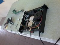
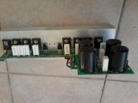
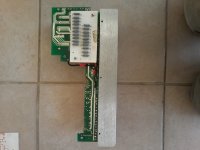
Here are some photos of the real thing. There is also a photographs of the high voltage test setup. The photo was taken during the test.
a) High voltage test for ten minutes: Passed.
b) Leakage test: supply rails to heatsink: Passed.
Estimated insulation resistance is 300 megaohms. This is based on the measuring instrument's resistance.
Here are some photos of the real thing. There is also a photographs of the high voltage test setup. The photo was taken during the test.
Attachments
 Its good when a plan comes together.
Testing for signal processing using a much simpler input stage and VAS resulted in 22A being drawn into the amplifier output stage. The testing voltage was +/-15V DC. The fault condition was caused by a faulty VAS transistor and an incorrect bias voltage. This is telling me that no amount of caution is an exaggeration. Since the test voltage was low the output stage did not sustain any damage.
I am at the stage of purchasing the VAS's, cascode and input current source's high voltage transistors. The problem with these is they are hard to find and in these cases one can easily end up asked for more money than the actual market price. I am cautious about using ebay fot the latter reason.
These transistors must a) support a high Vce voltage (>= 200V), a low Ic (max) that is in the range of 100mA to 50mA and a sufficiently high cutoff frequency (>= 150MHz).
During my simulations phase using LTSpice I found that using high current VAS transistors leads to great instability effectively turning the amplifier into a frenzy of oscillations. This also holds for the input stage.
I am on the lookout for transistors like these:
i) 2SC3600
ii) MJE340
iii) 2SA1406
Old CRT based television sets used to have video output driver transistors with similar characteristics. I am writing here because I do not know whether these can be used instead, provided they give the same or better performance.
P.S.
These are CRT video output transistors. My memory is not the same as it used to be.
Last edited:

I found the five transistors I still need to finish assembling the PCB housing the input, VAS, VBE multiplier and output overload protection circuit.
These are:
i) Input cascode transistors: MPSA44
ii) Input stage's current source transistor: MJE340
iii) VAS's current source's transistor 2SC3600
iv) VAS's amplifier transistor: 2SA1406
I have never analysed the circuit for noise which is motivating me to search for how-tos as noise is an unwanted ingredient. What I understand is, that noise, is generated at every temperature, at which electrons move randomly. I cannot speak of what happens when electrons have very low energy levels, at which point, they group and a conductor becomes superconductive.
Attachments
Last edited:
Hope it all performs as expected
Noise can be estimated in LTspice. Have a look in the LT help topics for starters.
Bob Cordell's book 'Designing Audio Power Amplifiers' has lots of info on this kind of thing and explains how to work back from raw figures of xxx μV RMS to a SNR in db.
Noise can be estimated in LTspice. Have a look in the LT help topics for starters.
Bob Cordell's book 'Designing Audio Power Amplifiers' has lots of info on this kind of thing and explains how to work back from raw figures of xxx μV RMS to a SNR in db.
Attachments
The input+VAS+VBE multiplier+output overcurrent limiter PCB will be connected to the output stage with 5 wires for the signal and 3 wires for the power supply. The wires carrying the signal are from an old IDE disk ribbon cable. I will be using a six wire ribbon. Using short wires for the interconnection seems to be the best option to minimize parasitics. However, using longer wires makes mounting easier and inspection in the event of a fault more accessible.
Should I opt to use longer wires for the interconnection? All wires will be kept together using tie wraps. The wires will be under a foot long if I opt to use long wires.
Should I opt to use longer wires for the interconnection? All wires will be kept together using tie wraps. The wires will be under a foot long if I opt to use long wires.
I found the five transistors I still need to finish assembling the PCB housing the input, VAS, VBE multiplier and output overload protection circuit.
These are:
i) Input cascode transistors: MPSA44
ii) Input stage's current source transistor: MJE340
iii) VAS's current source's transistor 2SC3600
iv) VAS's amplifier transistor: 2SA1406
I have never analysed the circuit for noise which is motivating me to search for how-tos as noise is an unwanted ingredient. What I understand is, that noise, is generated at every temperature, at which electrons move randomly. I cannot speak of what happens when electrons have very low energy levels, at which point, they group and a conductor becomes superconductive.
Where did you get 2sa1406/2sc3600 from???
What was their price?
Are these really genuine Sanyo?
Thank you,
cheers,
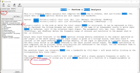
Further Analysis:
Douglas Self's book on amplifier design, talks about distortion in the input current despite the input voltage may seem unaffected. Remembering this, I analysed the input current waveform for distortion. The distortion figure is a delightful 0.001914% at 1KHz.
However, I also found the differential pair base currents have some temporary ringing. The VAS's amplifying transistor (PNP) does not suffer from any ringing.
These are the results:
N-Period=9
Fourier components of I(r13)
DC component:1.42735e-007
Harmonic Frequency Fourier Normalized Phase Normalized
Number [Hz] Component Component [degree] Phase [deg]
1 1.000e+03 1.307e-04 1.000e+00 -174.11° 0.00°
2 2.000e+03 1.915e-09 1.466e-05 124.17° 298.28°
3 3.000e+03 4.140e-10 3.168e-06 -110.28° 63.84°
4 4.000e+03 4.757e-10 3.641e-06 -102.66° 71.45°
5 5.000e+03 1.096e-09 8.386e-06 -150.55° 23.57°
6 6.000e+03 1.926e-10 1.474e-06 -119.04° 55.07°
7 7.000e+03 7.601e-10 5.817e-06 -139.71° 34.41°
8 8.000e+03 1.467e-10 1.123e-06 -107.96° 66.16°
9 9.000e+03 5.930e-10 4.538e-06 -137.08° 37.03°
Total Harmonic Distortion: 0.001914%(0.000000%)
P.S.
Some parts have arrived and the rest are shipped. The amplifier circuit should be complete in a few days for the initial testing with a low voltage power supply. I will use +/-18V DC at first, and then, I will use the full +/-85V DC but through high power (~200W) filament lamps.
Last edited:
- Home
- Amplifiers
- Solid State
- My attempts at a design of a 3 stage amplifier