Have a look at the classic academic paper by James E. Solomon (link to pdf) and published forty four years ago. Notice equations (15) and (18) which suggest an easy way to estimate the gain bandwidth product and the slew rate, just by inspection.
Applying those two equations to the LTSPICE schematic from post #178 (Figure 1 below), we find that estimated gain bandwidth product is approx 330 MHz and estimated slew rate is approx 54 V/usec . However it does seem likely that the output stage poles (which Solomon cheerfully assumes are negligible) are going to be at frequencies WELL below 330 MHz, driving phase margin to zero [marginal instability] or even to negative numbers [oscillation!].
Solomon says: you need to modify the design in some way, to make equation (15) predict a gain bandwidth product that is closer to what an amateur can achieve with low cost transistors and minimal test equipment. Make the front end bandwidth low enough that the output stage poles truly ARE negligible, as Solomon assumes.
I suggest: Swallow your pride and shoot for 20 million radians/second (3.2 MHz) of estimated gain bandwidth product instead. You have an excellent chance of hitting this less aggressive target, and in exchange for reduced machismo, getting a much more stable amplifier as a result.
Attachments
Last edited:
I've had a play with edbarx's design but it seems to defy conventional attempts to tame this behaviour completely.
I got it down to this and with the biggest change being seen in reverting to a conventional bootstrapped load for the VAS.
I got it down to this and with the biggest change being seen in reverting to a conventional bootstrapped load for the VAS.
Attachments
Another possible reason that I suspect is the phase of generated 2H (with pnp input and npn VAS combination) being preferred on listening evaluation, but I only find people discussing phase of 2H in Pass forum. Probably the effect is becoming less relevant when THD is lower than 0.01%....I've always thought one reason was that using PNP for the front end usually allows for an NPN VAS stage following, and usually high voltage high gain NPN's are much more readily available and better performing.
If the amplifier has a single ended power supply (+V and GND only), and if it uses the folded cascode topology, then a PNP / PJFET / PMOS input pair means the folded cascode is referenced to Ground, which has (by definition!) infinitely good power supply rejection.
Similar advantages accrue to 3-stage Blameless amplifiers with single supply and PNP inputs; the compensation capacitor is now referenced to Ground, so the amplifier's PSRR is a lot better.
A famous example of an amplifier using a single ended power supply is the Pass ACA sold here in the diyAudio store.
Quoting from the attached pdf.
Wh = gm1/Cc ................(15)
dVo/dt = 2Ic/Cc .............(18)
With:
2Ic = 2.6mA
gm1 = 5.8mS
Cc = 100pF
Wh = 5.8x10^-3/100x10^12 = 58x10^6Hz
dVo/dt = 2.6x10^3/100x10^12 = 26x10^6V/s
P.S.
Plotting Idiff/(Va - Vb) I got 47.7mS. Va and Vb are the voltages at the bases of the differential pair and Idiff is the current taken as output from the differential pair.
This is what this "proud" person gets from these formulae. Please, note I am not the kind of person who is convinced the universe revolves around them; I am too old and too tried to hold such a delusion.
Last edited:
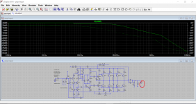
I've just noticed the sim still includes the capacitor loading on the output.
More weirdness now. If you run an AC analysis with the cap removed then the results are nuts.
So in sequence.
1/ This has the cap removed and no load attached.
2/ The cap removed. The load is attached.
3/ The load is now 10 meg. Cap still removed.
4/ The load in now removed.
Why is '4' not the same as '1' ?
What would you do with this amp Mark ?
Attachments
Wh = 5.8x10^-3/100x10^12 = 58x10^6Hz
Almost right; equation (15) gives a result in radians/sec ; to convert to cycles/sec ("Hertz"), divide by 2*Pi.
And you get gain bandwidth product of 9 Megahertz. In my opinion that's awfully aggressive for a hobby project using minimal test equipment. In post #201 I offered the suggestion that 20 megaradians/sec (3.2 Megahertz) might be a realistically achievable goal.
But I have to remind myself that Craig Breedlove was a hobbyist too, and yet he broke the world record for land vehicle speed several times, in jet engine powered cars that he built himself. link Just because someone's a hobbyist doesn't mean they can't be the very best in the world at a certain job.
_
Attachments
I kept record of many versions of the same amplifier just in case I arrive at a point of scrapping everything to start afresh. Whatever I do, the circuit will still remain a three stage amplifier which will consist of a differential input, VAS and power stage. So, my strategy is to keep record of everything, so that, I may be able to use parts that I know they work. The same can be said about writing software. If you know a certain set of functions work as expected, it would be useless to throw them away just because a project using them is far below expectations.
I think there is a good chance that the gain of the first stage is a lot less than you expect. That gain is gm_diffpair * (DiffPairRo // CurrentMirrorZout // StageTwoZin) and I think at least one of those terms might be surprisingly low.
It'd be easy to find out in an .AC analysis simulation; just plot the expression V(MirrorCollector)/(V(Q1base,Q2base)) and presto, that's the gain. Vout/Vin.
Possibly you might want to also double check the gain of the second stage while you're at it. It may well be that the output stage's Zin, is quite a hefty load for the second stage to drive without intermediate buffers/followers. What books call "drivers". Thus gain = gm_VAS * OPS_Zin , may be disappointingly small. Worth investigating.
The last few replies clearly give the impression my journey-adventure in designing a high power amplifier is a waste of time. This, to the extent, of suggesting throwing away everything and start afresh. I was told to undress my pride. This journey is not the result of pride. It is the result of a need to reuse a powerful power supply complete with a beautifully finished amplifier metal box.
I chose the hard way but courage sometimes can be seen as excessive and disproportionate pride.
I chose the hard way but courage sometimes can be seen as excessive and disproportionate pride.
The last few replies clearly give the impression my journey-adventure in designing a high power amplifier is a waste of time.
No, no no
") It is never that because you learn so much along the way.
It is never that because you learn so much along the way.Way back in this thread I suggested that you should first draw up your own specification for what you want. Distortion, bandwidth, how good do want it to be under squarewave testing, how tolerant of reactive loading. All those kinds of things.
Unless you do that you can be constantly trying to change things that already meet or exceed your goals.
You want to keep your basic output stage so try sticking a more conventional front end on to begin with.
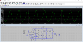
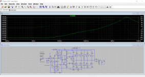
I never before this time did an AC Analysis, frequency response analysis, with the feedback loop disconnected. The test show the dotted line crosses the -180 degrees at around 80kHz. This is definitely bad and may be the reason for instability.
Since the latest circuit was deemed inadequate, I am doing my testing on this one which is still a works in progress.
Since the latest circuit was deemed inadequate, I am doing my testing on this one which is still a works in progress.
Attachments
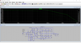
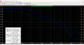
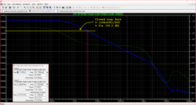
I don't know whether Mjona's open loop frequency response plot is representative of a design that is constantly being modified. But if we consider it a "snapshot" and study the plot a bit, we see its open loop gain is perhaps a bit low for an amplifier whose closed loop gain is 34dB. I drew a yellow line and a pink line on Mjona's plot.
_
_
Attachments
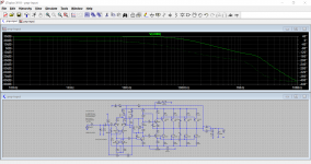
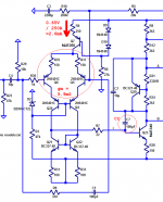
I have abandoned that plot which was based on using MJL21193/21194 outputs which I can see is not going to happen. Attached is an updated simulation using MJL1302/3281.
I have stuck with Bob Cordell's .models since these are accessible through the link to his site in the .inc statement.
That way anyone can run the simulations without having to change say MJL1302_Cordell to MJL1302C.
Anyway I am attaching my latest simulation. In the previous ones I had relied on C6 for compensation with different values (just showing to illustrate only). If MJE243/253 are up to the job with 85 volt supply rails these will give better stability margins than MJE340/350 which look a bit skinny to me.
I have not gone to a lot of length with this simulation so feel free to knock into whatever shape.
Attachments
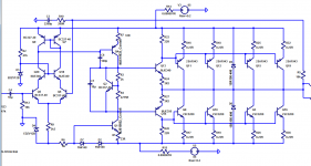
I have eight 2SC5200 and another eight 2SA1943 transistors already mounted on heatsinks with the driver and power stage shown. These were taken from a large public address amplifier (Wharfedale S1500). Since the amplifier failed and it was quite new but with the warranty period expired, I do not want to throw away everything. The amplifier's box contains a large powerful power supply that can supply about 15A of DC current at +/-85V. It has a beautiful finish, and in my opinion, it would be a waste to throw away everything. This is why I am keeping the power stages and power supply. I am only changing the pre-driver circuitry and the way the amplifier was grounded. I want the 0V rail to be grounded.I have abandoned that plot which was based on using MJL21193/21194 outputs which I can see is not going to happen. Attached is an updated simulation using MJL1302/3281.
Since the voltages are +/-85V, Vceo must be over 170V. This applies for the VAS's transistors. The other high voltage transistors need not be that high voltage although preferably they should be capable to withstand 170V in the event of a failure.
- Home
- Amplifiers
- Solid State
- My attempts at a design of a 3 stage amplifier