Sounds good. I'll check the voltages across the four 0.22 ohm resistors a little later and report back.
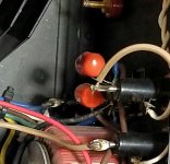
Funny you ask about a relay. That's one thing that I haven't looked very closely at. I don't have the amp in front of me now, but here's a so-so pic (below the top fuse holder in the photo) from the inside. Again, I'll take a look later to see how it's wired in, confirm continuity, etc.
Funny you ask about a relay. That's one thing that I haven't looked very closely at. I don't have the amp in front of me now, but here's a so-so pic (below the top fuse holder in the photo) from the inside. Again, I'll take a look later to see how it's wired in, confirm continuity, etc.
Attachments
Its a bit hard to decipher that from a picture tbh.
A pretty definitive check is to switch the amp OFF and then check for continuity from the positive speaker post back to the 0.22 ohms. With no relay present, both channels should have continuity. If one does and one doesn't then look for fuses and breaks in the wiring.
If there is a relay then the good channel (and the bad) will read as no continuity back to the 0.22 ohms.
The negative speaker post for both channels should connect to the amps main power supply ground or zero volt line.
You couldn't tell anything about that relay from my fantastic, detailed, close-up photo? ")
Well, it appears to be for power-on/off only, with no connection to the speakers. I verified by doing as you suggested and, with power off, testing for (and getting) continuity between the positive speaker terminals and the junctions of the 0.22 ohm resistors for both channels. So no speaker protection relay and no hidden fuses.
Here are my measurements across the 0.22 ohm resistors:
LEFT
K135 (top): +0.3mV
K135 (bottom): +0.2mV
J50 (top): +0.5mV
J50 (bottom): 0mV
RIGHT
K135 (top): +41.2mV
K135 (bottom): +3.0mV
J50 (top): +39.6mV
J50 (bottom): +3.3mV
I honestly couldn't get a relay of any kind out of the piccy Working from pictures is always difficult because you don't get any perspective or depth. Once you have seen it for real the picture would make sense... if you see what I mean.
I see the transformer, the red speaker post that may not even have a wire connected to it and two fuseholders, the upper one having a blue wire that has been snipped and a white wire that loops back on itself.
The readings...
The working channel appears to be biased to just under 200ma but the FET's are not sharing the current equally. That's another issue and tbh FET's from the same batch should be a lot closer than that. Nothing you can do at this time about that though.
The faulty channel is not drawing current and it should be.
The big question is what is going on here, because on a working amplifier (any amp FET or normal transistor) no bias current does not stop the amp working in any way.
Lets stick with this issue as it is something definite to work with. Also, we don't assume anything when fault finding, we look at every possibility.
So...
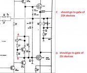
1/ Can you visually look at the FET's and confirm they are all marked correctly. Do any look to have been replaced. Ideally all batch numbers on like for like devices should be the same.
2/ The voltage between points A and B (which is effectively across collector and emitter of the transistor) should vary as you turn the bias preset.
3/ The voltage across the 150 ohm (points C and D) should also vary as you turn the preset. Points C and D go to FET gates (via the 220 ohm 'gate stoppers)
Setting the voltage across the 150 ohm in the bad channel to equal that of the good channel should give similar bias currents. Adjust slowly and keep feeling the FET's to make sure they do not start to get to hot.
Lets see what happens when you try and adjust it.
Working from pictures is always difficult because you don't get any perspective or depth. Once you have seen it for real the picture would make sense... if you see what I mean.I see the transformer, the red speaker post that may not even have a wire connected to it
and two fuseholders, the upper one having a blue wire that has been snipped and a white wire that loops back on itself.The readings...
The working channel appears to be biased to just under 200ma but the FET's are not sharing the current equally. That's another issue and tbh FET's from the same batch should be a lot closer than that. Nothing you can do at this time about that though.
The faulty channel is not drawing current and it should be.
The big question is what is going on here, because on a working amplifier (any amp FET or normal transistor) no bias current does not stop the amp working in any way.
Lets stick with this issue as it is something definite to work with. Also, we don't assume anything when fault finding, we look at every possibility.
So...
1/ Can you visually look at the FET's and confirm they are all marked correctly. Do any look to have been replaced. Ideally all batch numbers on like for like devices should be the same.
2/ The voltage between points A and B (which is effectively across collector and emitter of the transistor) should vary as you turn the bias preset.
3/ The voltage across the 150 ohm (points C and D) should also vary as you turn the preset. Points C and D go to FET gates (via the 220 ohm 'gate stoppers)
Setting the voltage across the 150 ohm in the bad channel to equal that of the good channel should give similar bias currents. Adjust slowly and keep feeling the FET's to make sure they do not start to get to hot.
Lets see what happens when you try and adjust it.
Attachments
Hi.
Seems to be something strange going on here.
The outputs should draw about the same current among the pairs and I won't belive that matching would be that bad, or has someone swapped them around?
Probably they're OK because they usually go shorted when faulty.
Do we have a offset measurement ?
It's possible that only one half is on followed by big offset.
Their Vgs determine the voltages on both sides of R38 referenced to ground so it's normal that they differ.
But voltage across should be about the same for a given bias.
I saw that there were sockets for the mosfets.
Are they OK ? I had problems with contact on my Altec 9440.
Figge.
We do have a DC offset measurement but I also agree that something very odd is going on. The gate bias voltage we have now (for the bad channel) should still be allowing significant current to flow.
Although no bias will not affect the amplifier operation (apart from a rise in distortion) it does seem to be a 'real' problem on this amp that we can look at and see why there is no bias. That in turn might lead to seeing why there is no audio output.
One other thing... can you hear any hiss/hum/noise from the bad channel once a speaker is connected ?
At the moment all the pieces to the puzzle aren't adding up... but they will hopefully in the end.
but I also agree that something very odd is going on. The gate bias voltage we have now (for the bad channel) should still be allowing significant current to flow. Although no bias will not affect the amplifier operation (apart from a rise in distortion) it does seem to be a 'real' problem on this amp that we can look at and see why there is no bias. That in turn might lead to seeing why there is no audio output.
One other thing... can you hear any hiss/hum/noise from the bad channel once a speaker is connected ?
At the moment all the pieces to the puzzle aren't adding up... but they will hopefully in the end.
One reading that can be inferred but needs checking is that voltage on L1 is zero. The driver voltages suggest it will be but you should check.
As for L1, yes, the voltage is zero.
Let's see...
1. The FET's all appear to be from the same batch. For the J50's, each has the Hitachi symbol and 0A2. For the K135's, each has the Hitachi symbol and 0C2. That said, Trollet is correct about one of the sockets being different: The top one for the J50 on the left channel is different.
2. The voltage between points A and B does vary when I turn the bias preset.
3. The voltage between points C and D, across the 150 ohm resistor (R38), also varies when I turn the bias preset. When the voltage between A and B was at +2.96V, it measured +1.64V between A and B, fwiw.
Confession time: I've been going by the owner's report regarding there being no sound out of the left channel. Yes, I should not have assumed that to be correct. I'll confirm later on.
No problem I've been a service tech far to long in a past life. Never believe the customer
The bias control voltage seems to vary OK and so you should be able to get the FET's to conduct the required bias current (by measuring the tiny voltage dropped across the 0.22 ohms).
I've been a service tech far to long in a past life. Never believe the customer The bias control voltage seems to vary OK and so you should be able to get the FET's to conduct the required bias current (by measuring the tiny voltage dropped across the 0.22 ohms).
I guess the operative word here is "should." Turning the bias preset has no effect on the voltage across the 0.22 ohm resistors when I checked them at the two K135's.
Here's something else anomalous: When I measure the voltage before the 220 ohm resistor at the FET gate of the top J50 (left channel still), I get the same figure I measure where the wire exits the PCB: 0.991V. But right after that resistor, and before its soldered to the socket terminal for the gate, I get -0.551V. For the corresponding J50 on the other side, the voltages are approximately the same before and after (as I see they are at the other 220 ohm gate resistors). I had earlier noticed this voltage difference at this specific resistor, and went ahead and replaced it, but it seems the resistor isn't the problem. Could this indicate a short of some kind with this J50?
Here's something else anomalous: When I measure the voltage before the 220 ohm resistor at the FET gate of the top J50 (left channel still), I get the same figure I measure where the wire exits the PCB: 0.991V. But right after that resistor, and before its soldered to the socket terminal for the gate, I get -0.551V. For the corresponding J50 on the other side, the voltages are approximately the same before and after (as I see they are at the other 220 ohm gate resistors). I had earlier noticed this voltage difference at this specific resistor, and went ahead and replaced it, but it seems the resistor isn't the problem. Could this indicate a short of some kind with this J50?
The gate of a FET should draw no measurable current at DC which means that the voltage on the 220 ohm should be the same on both sides...
So something odd going on.
The important voltage is the voltage present between the two gates (across that 150 ohm) as that determines whether the FET's conduct. The absolute value is less important.
For example if the gate of each FET were at 19 volts then no current would flow. Make the upper FET gate 19 and the lower FET gate 17.5 and significant current would flow. You would also have a DC offset under those conditions but that is just to illustrate it is the voltage difference between the gates rather than absolute voltage that determines the conduction.
Your readings show something is happening though. On the diagram I drew above, whatever voltage is between points C and D should also be seen across the FET gates which are after the 220 ohms.
One important point, the 220 ohms are to stop instability and oscillation (they are called parasitic gate stoppers) and so it possible the very act of placing the meter lead on the FET gate is causing instability which in turn would alter the reading.
If that were the case then you would expect other noticeable effects such as heat being generated as the thing broke in oscillation. In the absence of a scope we can still make a valid reading by tagging a resistor to each gate terminal and connecting the meter to the end of each resistor. Just do that for one pair of devices. They would isolate the FET from the meter and allow a true reading. 10k, 22k, anything like that would be good.
I'm still suspicious about that socket.
If the gate has contact with the heatsink it won't draw any current and it will drop X volts over 220R.
Bad contact will cause other problems.
All measurements on driver cirquit indicates that it works so I would have pulled the fets with strange values and checked them and the sockets.
Figge
If the gate has contact with the heatsink it won't draw any current and it will drop X volts over 220R.
Bad contact will cause other problems.
All measurements on driver cirquit indicates that it works so I would have pulled the fets with strange values and checked them and the sockets.
Figge
That green TO3 socket does look badly fitted , all the heat sink paste on the wrong side is it there to fill a gap ? ie ..the socket is not fitting flush with the heat sink . In the 2nd photo can i even see the hole in the heat sink that the socket should be covering that would suggest the gate could indeed be in electrical contact with the heat sink as Trollet is suggesting .
Mooly: I do have a scope, if that would be a better option for checking the FET without the potential for oscillation caused by the meter. Or as I've already pulled one (see below)....
Trollet and epicyclic: I pulled the transistor from the suspect socket this a.m., but before doing so checked to see if there was any continuity between the gate and heat sink. There wasn't. I'm still not crazy about the fit of that socket, so I'll transfer the connections to a new one, clean the thermal grease from the socket mounting side, and also replace the insulators between the heat sink mounting holes and transistors. I'd like to test this FET while I have it out, but unfortunately my ancient/primitive Micronata dynamic transistor tester doesn't provide any instructions for checking FETs (so I assume I can't). Any recommendations for alternate method?
Trollet and epicyclic: I pulled the transistor from the suspect socket this a.m., but before doing so checked to see if there was any continuity between the gate and heat sink. There wasn't. I'm still not crazy about the fit of that socket, so I'll transfer the connections to a new one, clean the thermal grease from the socket mounting side, and also replace the insulators between the heat sink mounting holes and transistors. I'd like to test this FET while I have it out, but unfortunately my ancient/primitive Micronata dynamic transistor tester doesn't provide any instructions for checking FETs (so I assume I can't). Any recommendations for alternate method?
If you dangle the scope on the main output (L1 etc) then you should not see any oscillation.
Measure the voltage across the 150 ohms and note the value, then transfer the meter leads to the other end of the 220 ohms (do two sets of measurements, one for each set of 220 ohms) and see if the reading is identical. It should be. If not then look at the scope and see if any oscillation is present as you attempt to measure directly on the FET's. If there is then that is why the reading changes and seems weird.
Lateral FET's are extremely robust and would normally fail either short circuit or very leaky which would be obvious (fuses blowing etc). We need to conclusively prove that you are getting this 1.4 volts DC bias voltage between the gates and that with that present there is no current flowing in the 0.22ohms. That then leaves the possibility of a weird failure mode in the FET's or some undiscovered connection/socket issue.
I also can't help thinking of the good channel and the very unequal current sharing between the two pairs. That suggests that one of the pair on that channel isn't doing what we would really expect. Each channel will work normally with just a single pair fitted and so that could be a possible way to test the devices although normally swapping parts between channels isn't a great idea... however...
I didn't replace the socket for that J50, but I did clean it up and reinstall the FET paying attention to positioning with respect to the heat sink. The insulating sleeves are in place and no shorts were found.
Well, there was no oscillation evident when I measured across the 150 ohm (R38) and then across the two pairs of gates.
R38 (150 ohm)
+1.28V
K135 gates
0.00V
J50 gates
+0.470V
Could the 33pF capacitors between the gate and drain of each K135 be playing any role? Or the 0.1uf? Yep, I'm grasping at straws here.
The three 0.1's (C15, C21 and C23) would not cause this problem. If C15 was open circuit then the amp might be unstable but the scope is saying no.
The 33pF. I'd have to say no for the simple reason that even if one of them were faulty (leaky or short circuit), you would still have the 1.28 volts applied to the other one and that FET pair would work normally.
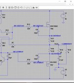
I've changed a simulation I had of a lateral FET amp to match your output stage. This is what you should be seeing. Do you see how the FET gates draw no current. There is no volt drop across the 220 ohms. The voltage between the 220 ohms should be identical at the left and right sides (your 1.28 volts). That kind of voltage causes around 200ma to flow in the lateral FET's. You should be seeing similar to this on each parallel pair of FET's.
(Ignore the 33pF on the lower FET as the designer hasn't fitted them on the lower P channel FET's.)
The 33pF. I'd have to say no for the simple reason that even if one of them were faulty (leaky or short circuit), you would still have the 1.28 volts applied to the other one and that FET pair would work normally.
I've changed a simulation I had of a lateral FET amp to match your output stage. This is what you should be seeing. Do you see how the FET gates draw no current. There is no volt drop across the 220 ohms. The voltage between the 220 ohms should be identical at the left and right sides (your 1.28 volts). That kind of voltage causes around 200ma to flow in the lateral FET's. You should be seeing similar to this on each parallel pair of FET's.
(Ignore the 33pF on the lower FET as the designer hasn't fitted them on the lower P channel FET's.)
Attachments
- Status
- This old topic is closed. If you want to reopen this topic, contact a moderator using the "Report Post" button.
- Home
- Amplifiers
- Solid State
- Borbely DC 100 Amp: Left Channel Troubleshooting