Given all the talk about damping factor, I am trying to understand how the choice of certain transistor parts control the damping factors. How does that work, and why?
Damping factor is related to output impedance of amplifier. The natural open loop output impedance is reduced by the feedback factor. feedback factor is the ratio of open loop gain on the close gain. Open loop gain is the multiplication of each gain stage. Each gain stage is a function of resistor loading. Resistor loading value is based on the bias voltage required for the next stage. Higher bias voltage threshold ( VGS of mosfet or VBE of bjt) results in higher loading resistor value for the preceding stage. Also, Jfet input stage have their current related to their source resistor value. Even output bias current provides different transconductance thus affects high open loop gain. This is a cascading effect and you need to balance it all.
The problem with original F5 topology to use lateral mosfet ( Ex: Profet amplifier) which gave a too low DF (< 10) has been fixed with the USSA type topology. Pass approach was to use positive feedback in the F7 to increase DF with lateral. But this is tricky to play with positive feedback.... Also the driver stage of the USSA provides advantage. Also the almost non existing output mosfet source resistor (very low value such as 0.01 ohms ) gives increased square law effect of class A compared to 0.47 ohms source resistor.
Fab
Last edited:
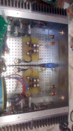
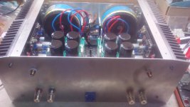
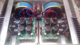
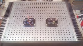
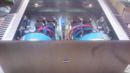
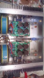
USSA-3
Thanks danny_66")
See post 1 of this thread :
USSA-3B new Version based on USSA-3
Now I have a new version under listening test and another future possible one for AnthonyA...
Here is the summary:
USSA3.0 : jfet input, mosfet driver and lateral mosfet output stage (original version)
USSA3B : jfet input , bjt driver, bjt output
USSA3.1 : jfet input, bjt driver, lateral mosfet output (under listening)
USSA3B.1: jfet input, mosfet driver, bjt output (not done yet)
I realize that now several peoples intend to build another variant from original USSA3.0 thus I need to add this info soon into the USSA3 build manual...
Fab
Nice Fab!
I was just picking up my USSA3 build after finishing some other projects and now there is a version 3.1
Do I understand correctly that it is the same input and driver stage as the 3,
but with bipolars instead of laterals for output ?
Thanks danny_66
See post 1 of this thread :
USSA-3B new Version based on USSA-3
Now I have a new version under listening test and another future possible one for AnthonyA...
Here is the summary:
USSA3.0 : jfet input, mosfet driver and lateral mosfet output stage (original version)
USSA3B : jfet input , bjt driver, bjt output
USSA3.1 : jfet input, bjt driver, lateral mosfet output (under listening)
USSA3B.1: jfet input, mosfet driver, bjt output (not done yet)
I realize that now several peoples intend to build another variant from original USSA3.0 thus I need to add this info soon into the USSA3 build manual...
Fab
Last edited:
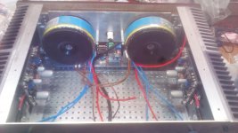
Results
For my sanity please comment.
Right Channel
VGSP = 1.504V Measured total R = 66.7 ohms IM3 = 22.55mA
VGSN = 0.914V Measured total R = 39.9 ohms IM4 =22.9mA
Left Channel
VGSP = 1.67V Measured total R = 73.8 ohms IM3 = 22.63mA
VGSN = 1.06V Measured total R = 47.3 ohms IM4 = 22.41mA
Power supply at amp PCB +/-23.1Volts
Power supply before ripple eater +/- 26.2Volts
Bias = 70mV
Offset
Short circuit input = 0.3mV
Open circuit input = 7mV
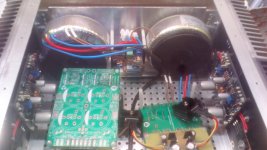
A couple of setbacks, I bumped one of the 2,200uF caps and it seems that I damaged it as it feels loose on the PCB. Not sure if I can buy one locally.
Also there is a slight “buzz” coming from the transformers, which I do not get from my other amps. Perhaps it’s the way I have mounted the transformers, vertically, or the brand that I bought. Unfortunately I currently don’t have the time to investigate.
For my sanity please comment.
Right Channel
VGSP = 1.504V Measured total R = 66.7 ohms IM3 = 22.55mA
VGSN = 0.914V Measured total R = 39.9 ohms IM4 =22.9mA
Left Channel
VGSP = 1.67V Measured total R = 73.8 ohms IM3 = 22.63mA
VGSN = 1.06V Measured total R = 47.3 ohms IM4 = 22.41mA
Power supply at amp PCB +/-23.1Volts
Power supply before ripple eater +/- 26.2Volts
Bias = 70mV
Offset
Short circuit input = 0.3mV
Open circuit input = 7mV
A couple of setbacks, I bumped one of the 2,200uF caps and it seems that I damaged it as it feels loose on the PCB. Not sure if I can buy one locally.
Also there is a slight “buzz” coming from the transformers, which I do not get from my other amps. Perhaps it’s the way I have mounted the transformers, vertically, or the brand that I bought. Unfortunately I currently don’t have the time to investigate.
Hi Harry3
Your results seem correct.
I can imagine that you must be angry with the damaged cap....
As for the transformer, you have 1.4 A bias current so you need a good transformer. I know I had a 180VA from Summer doing a slight mechanical buzz at 1.3A but was not audible with amplifier cover on. You can try to rotate it to see the effect and have some soft material doing some damping between transfo and chassis. I use 250VA medical Triad transformer for my USSA5 at 1.3A bias and not any sign of buzz present.
Fab
Last edited:
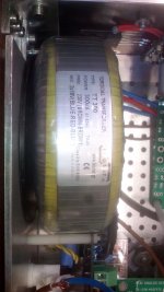
I'm using 300VA Vigortronix from Element14, for each channel, so the 1.4amp bias should not be a problem.
I will try and re position the transformers but I didn't have any issues like this when I bought locally assembled transformers for my other amps. When I get time I will investigate.
I will try and re position the transformers but I didn't have any issues like this when I bought locally assembled transformers for my other amps. When I get time I will investigate.
Hi Anthony,
Thanks for your suggestions. I actually have a DC blocker PCB that I can build, just to eliminate that possibility but I think it's the two transformers that are the issue. Never a dull moment.
Hi Niko,
welcome back! Are you changing your power supply or is this a different build?
Regards
Harry
Thanks for your suggestions. I actually have a DC blocker PCB that I can build, just to eliminate that possibility but I think it's the two transformers that are the issue. Never a dull moment.
Hi Niko,
welcome back! Are you changing your power supply or is this a different build?
Regards
Harry
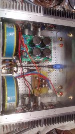
Free I fire it up, one channel after one year. Voltages after CRC are +/-24V . Output voltages ripple eater +/-22V at 1.3 A =65mv trafo 2X18V /300VA
I forgot to mention the ripple after CRC about 140mv pk-pk
I forgot to mention the ripple after CRC about 140mv pk-pk
Attachments
Last edited:
- Home
- Amplifiers
- Solid State
- USSA-5 Build with Review