Thank you guys, then I think I will also go via the dual mono build as already have couple of Universal PSU boards from diyaudio store fully populated with Panasonic caps.
Transformer 1:
PRIMARY : 0---230 VOLT. With Shield
SECONDARY :
0---19 V./ 5 Amp.
0---19 V./ 5 Amp
Transformer 2:
PRIMARY : 0---230 VOLT. With Shield
SECONDARY :
0---19 V./ 5 Amp.
0---19 V./ 5 Amp
")
Transformer 1:
PRIMARY : 0---230 VOLT. With Shield
SECONDARY :
0---19 V./ 5 Amp.
0---19 V./ 5 Amp
Transformer 2:
PRIMARY : 0---230 VOLT. With Shield
SECONDARY :
0---19 V./ 5 Amp.
0---19 V./ 5 Amp
Good luck Manniraj, hope you receive your transformers soon.
What chassis are you planning to use?
Thanks zman01, I am going to reuse my Sony VFET2 amp chassis for this build as it has sufficient spacing to place couple of transformers with 2 PSU boards.
Finally some progress
Hi folks
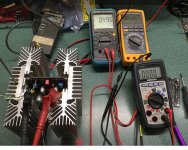
I am building a USSA5 from chassis and heatsink parts I have on hand. The result is unusual and is a very difficult mechanical assembly. Here is a photo of one channel assembly under test with bench supplies at roughly 25volts. Th heatsink assemblies are 5”high and about 7.5 inches long for each half of the output stage. I am testing this initially open air. The chassis these will be installed in will have about a 3 inch deep lower deck below the heatsinks where fans will be installed to provide cooling if required. I have 3 meters monitoring +- source resistor voltages and one for dc output offset. In the back left is a thermometer with the probe mounted directly behind the output mosfet. Right now it is up to 110F. DC offset is very stable with temperature shift. Hardly moves a mv from where it’s set. Perhaps that is helped by the regulated bench supply.
Fab, if you see this I have a question for you. The new changes to resistors implemented in 5.1 where the 4.7k resistors in series with the thermistors are changed to 1.5k- is that a change recommended for the 5 version?
Hi folks
I am building a USSA5 from chassis and heatsink parts I have on hand. The result is unusual and is a very difficult mechanical assembly. Here is a photo of one channel assembly under test with bench supplies at roughly 25volts. Th heatsink assemblies are 5”high and about 7.5 inches long for each half of the output stage. I am testing this initially open air. The chassis these will be installed in will have about a 3 inch deep lower deck below the heatsinks where fans will be installed to provide cooling if required. I have 3 meters monitoring +- source resistor voltages and one for dc output offset. In the back left is a thermometer with the probe mounted directly behind the output mosfet. Right now it is up to 110F. DC offset is very stable with temperature shift. Hardly moves a mv from where it’s set. Perhaps that is helped by the regulated bench supply.
Fab, if you see this I have a question for you. The new changes to resistors implemented in 5.1 where the 4.7k resistors in series with the thermistors are changed to 1.5k- is that a change recommended for the 5 version?
Attachments
Hi Bfpca
You have made good progress and your implementation seems a challenge. I would pay attention to ensure to not put too much pressure on transistors leads while moving the heatsinks ...
There is no change on the temperature compensation for the original USSA 5 version using the mosfet drivers. This version has been built so many times and without issues thus no changes needed.
The version 5.1 using bjt drivers is new but from latest implementation results the temperature compensation is perfect.
Fab
You have made good progress
and your implementation seems a challenge. I would pay attention to ensure to not put too much pressure on transistors leads while moving the heatsinks ...There is no change on the temperature compensation for the original USSA 5 version using the mosfet drivers. This version has been built so many times and without issues thus no changes needed.
The version 5.1 using bjt drivers is new but from latest implementation results the temperature compensation is perfect.
Fab
Ok, thank you Fab. The 2 heatsinks are joined on the bottom to 2 1/4” braces to keep them from shifting. The boards are mounted to the heatsinks with an angle bracket at each corner so the whole assembly is pretty rigid. It then mounts to the chassis via the braces.
I reached a temp equilibrium of 118F (48c) today at +-25volts 1.05 amps operating point. When mounted on the chassis I may get a slightly lower temp due to improved air flow. If it runs too hot I have fans that can be turned on to lower temp.
I was able to calculate the resistor values for the drivers and will install those and mount the assembly in the chassis and rebias to check the thermal performance again. I have the output mosfets mounted using Keratherm insulators purchased form the DIY store. These insulators are expensive but work really well and no mess installing them like thermal grease. I also drilled and tapped an additional hole on the heatsink above the thermistor. I placed a to220 insulator pad on the heatsink and then the thermistor with thermal grease. I then made a cover for it out of 1/4” phenolic that mounts like a transistor to the heatsink using the extra mounting hole and the thermal insulator pad. The underside of the phenolic has a hollow section for the thermistor. So the thermistor is in good thermal contact with the heatsink and is protected from air currents that could cool it. The insulator pad prevents any short circuits to the heatsink. I also put heat shrink on the thermistor leads to prevent any mishaps.
I need to order a few more parts from Mouser before I can finish the second board. I also need to work on some household projects so I am not sure when I will get to finish the amp.
You appear to have figured out a well integrated solution You effectively have created a stable heatsinks arrangement
For the thermistors installation it may appear overkill but with the fan air flow directly toward it it appears a good solution
Keep us posted on future progress.
Fab
You effectively have created a stable heatsinks arrangementFor the thermistors installation it may appear overkill but with the fan air flow directly toward it it appears a good solution
Keep us posted on future progress.
Fab
Last edited:
I have a very fundemental question.
Lets say my dac output is 1.6v rms,
If i use it with usspa or any smillar gain preamplifer
It will easly reach more voltaga than Input sensitivity of ussa5 (1.8v)
So i guess it will cause unstablity and clipping. Am i miss something here?
Lets say my dac output is 1.6v rms,
If i use it with usspa or any smillar gain preamplifer
It will easly reach more voltaga than Input sensitivity of ussa5 (1.8v)
So i guess it will cause unstablity and clipping. Am i miss something here?
Hi Fab
I just did soldering the boards with the parts and I have left out R5/6 which I think I need to solder it. I also need to solder RV1B=100R and RV2B=47R resistors before the initial measurement.
Regarding R15/16 I have soldered 0.05R 1w resistor as per the BOM and can I do this for the initial setup?

Thanks
I just did soldering the boards with the parts and I have left out R5/6 which I think I need to solder it. I also need to solder RV1B=100R and RV2B=47R resistors before the initial measurement.
Regarding R15/16 I have soldered 0.05R 1w resistor as per the BOM and can I do this for the initial setup?
Thanks
Last edited:
Sorry I was not notified about this post by email ...I have a very fundemental question.
Lets say my dac output is 1.6v rms,
If i use it with usspa or any smillar gain preamplifer
It will easly reach more voltaga than Input sensitivity of ussa5 (1.8v)
So i guess it will cause unstablity and clipping. Am i miss something here?
It is always a good practice to have an overall level higher than the sensitivity because your source level is always lower than the max indicated. From experience the recordings on different albums can have sometimes like about 12dB ( old recorded albums ) or so difference between each other
so for the low level recordings you will get much less power than possible. In a sound system I try to target at least 2 or even 3 times (6 to 10dB) the sensitivity level to get max power to cover all cases. For high level recordings you will notice when clipping occurs so you should not go for a very long time at that level. The USSPA with +/-12-18vDC can take a very high input signal and the USSA amps have soft clipping so no risk of problem there.
Fab
Last edited:
Hi manniraj
Good start.
Yes R15/R16 will not be biased without the output transistors installed as per figure 18 of the manual ( zener diode ) so it is ok.
Fab
Thanks Fab, then I am good to go with the initial setup as per your new manual. Some how missed to get the R5/6 resistors rated 10k 0.5W Vishay Dale during my BOM order from Mouser. Looking at locally now.
Regarding the below step mentioned in your manual, it says to use 100R and 47R 0.5W resistors for RV1B/2B before the initial measurement. So do you mean that this needs to be removed after the initial measurement?
For RV1B use 100 Ohms and for RV2B use 47 Ohms (as initial values before measurement)
Last edited:
Hi manniraj
If you follow the manual closely you cannot get it wrong. In the different test steps all resistors shown are required for testing. The exception is that R5/R6 can be temporarily omitted but I strongly recommend installing them to divide some of the input stage current outside the pot and when R5/R6 will be once installed then it will impose readjustment of the pots.....
And yes, if you read further in the manual you will see that RV1A, RV1B, RV2A and RV2B will probably need to be changed for the calculated resistors values to have about equal current in the positive and negative sides of driver stage. I recommend that you read completely the manual first before going further so you have an idea of the next steps in advance.
First test is to adjust the input stage current (CCS). Good luck.
Fab
Last edited:
A small update regarding my build. The first amp board started with the initial steps and completed till 8.8.5 successfully without any issues RV1B = 100R and RV2B = 47R as initial values along with the source power resistors which were already installed and as confirmed by Fab they do not come into the circuit without the mosfets.
I have now soldered the C5/6 caps, then Rz and Cz as well.
RV1B = 100R and RV2B = 47R as initial values along with the source power resistors which were already installed and as confirmed by Fab they do not come into the circuit without the mosfets. I have now soldered the C5/6 caps, then Rz and Cz as well.
The 2SK1058/2SJ162 mosfets are single die mosfet. Parallel option could theoretically work but would require these changes or challenges:
1) very close match between same channel mosfet because of the required very low source resistor value;
2) reduce by half each resistor value for each gate of mosfet and physically located very close to gate;
3) the pcb is for a single package thus would require to locate mosfet more away of the pcb which can cause parasitic issue;
In conclusion, much easier to get the good double die Exicon for this project and keep your single die mosfet for another project...
Fab
Because I have enough 2SK1058/2SJ162 mosfets, how about using these (parallel) instead ALF or Exicon?
Would change in part values or other mods be necessary?
Appreciate any input
How many do you have ?
- Home
- Amplifiers
- Solid State
- USSA-5 Build with Review