Max,
the need for compensation capacitor indicates a serious condition. I am not a fan of Japanese commercially made amplifiers.
Oh, sorry. I could have mislead you by quoting different amps and configurations.
SONY TA-5650 is a common-source push-pull VFET output amp, if I am rightly defining it, and the caps that I added are just power supply bypass (not compensation) caps from as near as the source pin I can to ground, as the SONY TA-N7 (cascoded VFET output; posted above) also shows. They can't hurt and they surelly can help to sound AND possibly to increasing stability margins, as the mains caps are very far away. The amp was created +/- in 1976 so it was stable...that being said, many are unstable and I am trying to solve that.
BTW, have you listened to one. They surelly have potential.
Thanks for your concern.
M.
Attachments
50µm is _massively thick_ gold plating, ten times more than "heavily gold plated" connectors. I think you mean 0.50µm plated.
50µm on AWG (radius about 200µm) would mean that 33% of the wire is gold (increasing the average resistivity of the wire somewhat!)
Indeed, I found the business card that states the 0.50um (0.5um) plating.
The wire is quite good. It has an organic and truthful sound and lots of bass amplitude and extension from a tinny wire. Brass instruments sound phenomenal. It allows the punch of the Amnesis to express itself. I braided 3 wires per side and it seems good enough.
I am thinking of using it also as internal wiring for my amps, apart from interconnects, that is.
Don't miss the promo prices.
Cheers,
M.
Attachments
Max,
That is common-source topology all right, in the absence of distinguishing definition (no need for it either). Bypass capacitor is a good thing, phase compensation capacitor is a bad thing.
indra1,
commenting post #631
Currents do not drive transistors, voltages do. What static induction transistors care about is the gate to channel voltage. The common-emitter topology is not unproblematic concerning driving capability, nor is the voltage follower.
Ripple voltage is a nonissue here, IC regulated power supplies and bootstrapping are generally objectionable.
The problem under paragraph 3) applies more or less to all topologies where the output is balanced to ground. The Hiraga amplifier follows the load variations closely, large energy shifts are damped by the intrinsic resistance, local feedback and global feedback besides the 1 ohm resistor. It is not the role of 8.2k resistors to drive the input capacitance. How on earth can a depletion mode device operate in enhancement mode? The description of the operation is regrettably flawed.
Yes, thermal abuse leads easily to damage or destruction. The thick silicon dioxide layer utilized results in low input capacitance, wide bandwidth, low sensitivity, low gate-to-source series resistance, but also in a decrease in reliability. I agree on the necessity of gate stopper.
The expression "dynamic balance" in this context is nonsensical, undesirable and unrealizable. Signal voltages approaching the supply voltage will be terribly distorted.
That is common-source topology all right, in the absence of distinguishing definition (no need for it either). Bypass capacitor is a good thing, phase compensation capacitor is a bad thing.
indra1,
commenting post #631
Mr Hiraga rather unwisely simply transposed his 'darlingnot' circuit which is current driven, into an attempt to make the current of the BJT driver stage into driving voltage for the SIT/VFETs. There are several problems with this:
Currents do not drive transistors, voltages do. What static induction transistors care about is the gate to channel voltage. The common-emitter topology is not unproblematic concerning driving capability, nor is the voltage follower.
1) A relatively minor problem is that the required bias voltage for a chosen bias current depends on the power supply voltage. In other words, any sag or ripple will modulate the bias current. The only logical solution that would keep the schematic simple, would be to regulate the power supply.
Ripple voltage is a nonissue here, IC regulated power supplies and bootstrapping are generally objectionable.
The problem under paragraph 3) applies more or less to all topologies where the output is balanced to ground. The Hiraga amplifier follows the load variations closely, large energy shifts are damped by the intrinsic resistance, local feedback and global feedback besides the 1 ohm resistor. It is not the role of 8.2k resistors to drive the input capacitance. How on earth can a depletion mode device operate in enhancement mode? The description of the operation is regrettably flawed.
Yes, thermal abuse leads easily to damage or destruction. The thick silicon dioxide layer utilized results in low input capacitance, wide bandwidth, low sensitivity, low gate-to-source series resistance, but also in a decrease in reliability. I agree on the necessity of gate stopper.
The expression "dynamic balance" in this context is nonsensical, undesirable and unrealizable. Signal voltages approaching the supply voltage will be terribly distorted.
I only wish to prevent unnecessary grief. Please do not pose arguments that could mislead unsuspecting potential builders, the SITs are very valuable and rare.... commenting post #631
The 2SK82 and 2SJ28 are vertical power Jfets so no silicon dioxide layer.The thick silicon dioxide layer utilized results in low input capacitance, wide bandwidth, low sensitivity, low gate-to-source series resistance, but also in a decrease in reliability. ...
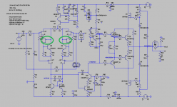
I am back with the following comments.
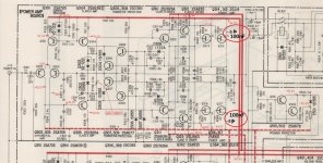
Zobel network
Without zobel network the amplifier oscillates at 7..2 0MHz.
To stop oscillation a resistor < 20 ohms has to be connected to the
output. The inductivity should be well below 1uH.
A resistor of 10 ohms and a capacitor of 47nF mounted directly to the
PCB is a good choice.
Stability
The problem with my test track 'Royal March' (see post #577)
does only occur if driver and output are cascoded/bootstrapped.
The problem does not occur with
- Darlington version (output cascoded/bootstrapped, no driver cascode)
- cascoded/bootstrapped driver, output transistors connected directly
to power rails (no MOSFET)
If I increase C10=100nF to 200nF in the VAS the stability of the
amp concerning my test track increases by a great amount. Increasing
additonally the Cap across the emitter resistors of the driver from
100n to 1-2uF the amp is stable.
I already mentioned that the problem does not occur for all versions if
input transistors Q3/Q5 (BC557C) are replaced by a p-JFET
(e.g. 2SJ103) which limits the bandwidth of the input stage so that the
rise time increases to 2us even without any input filter.
This option has the following advantages for me since
I use a DAC with very low offset and with passive volume control without output buffer:
- no input Cap required (sound coloration, high price, component volume)
- increased Input resistor (up to 100k)
- amp offset not dependent on source impedance
Listening Tests (JFET input with different output versions)
@Max
The amp sounds great in all versions
I am not so convinced of bootstrapping as you are.
At least in my audio chain / room acoustics the bootstrapping sounds a little pale and too fat in the mid bass region. It depends on the kind of music (my
focus is not classical music <20%).
So I will use no or only moderate caps in the driver / output section.
By inserting a switch for the VAS bootstrapping I can easily choose
between 2 different sounding amplifiers.
I compared the QUAD version to the Darlington version.
Both are sounding great. The Darlington version sounds less
voluminous / more detailed the QUAD more relaxed.
It needs more listening tests to decide which to use.
For people who want to design a less complex / more stable amp
I recoment the Darlinton version.
Power Supply
For many years I use an external CLC power supply (10.000uF-> 2mH
->22.0000uF) and I like it. Maybe I should reduce the inductivity.
AllBJT input
For the near future no tests are planned since I'm satisfied with the
more simpler JFET input.
Further listening impressions will follow.
Dear JOS1,
I've been thinking about our problem with the "Royal March" track and trying to figure out what to do...
So far I would guess increasing power supply so increasing headroom could lift the problem to a higher (not needed in real life) power requirement...
A Baker Clamp was recommended for the CCS loaded VAS but was neglected on the Bootstrap loaded VAS based on hearsay...maybe a Baker Clamp is also needed there (// to Miller cap) in the form of a small Schottky diode.
I once got rid of an oscillation problem on a QUAD by using a small inductor //R16-R40 (33Ohm) at the bases of drivers BJTs...mere chance maybe, but it worked. Maybe the same can be used at the base of the output BJT.
Random thoughts. I am not in the mood for DIY lately; it is cold out there.
But enjoying sweet music.
Cheers,
M.
Last edited:
Hi Max,
With this measure the amp is absolutely stable even without input filter
and any compensation in the driver / output section
("Royal March" track is no problem anymore)
The Zobel 10R/47nF is placed directly on the PCB, an inductance (1uH )
without 10R resistor is realized by some copper windings around the
speaker connector.
Your proposal the add a second JFET in the input section improves sound.
VAS section:
I prefer MPSA18 / 2SC4793.
100pF cap: Is the dielectric (ceramic, mica etc.) relevant for sound.
Any news concerning 47R resistor?
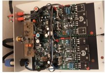
I built 2 mono blocks (ext. Power Supply) each consisting of 2 amps, one for the bass and one for the mid/high section for my 2way speaker.
I skipped the cross over network in my speaker and use passive Low Pass / High Pass filter (1st order) in front of both amps with small high quality caps.
So I can easily change crossover frequency and the speaker level by adapting the gain of the amps. This allows me to change the sound to my taste and
even compensate the room acoustics a little.
This improves sound by a great amount.
I regret that there are no further interested members to built this outstanding amp.
Since I am satisfied with the present amp (JFET input) I will finish this project at least for now. There are other components in the audio chain that need improvement.
Btw: I read somewhere that you own a MOSAIC USB DAC.
Are you satisfied with this new interesting DAC concept from ECdesigns. Is this the favorite DAC for your listening tests.
I think about ordering the new MOS16/MOS24 DAC with Toshlink input.
Do you have any experience with 96k/24Bit reproduction.
Keep me informed if you have any news about the Amnesis Amp.
I already mentioned that the problem does not occur for all versions if
input transistors Q3/Q5 (BC557C) are replaced by a p-JFET
(e.g. 2SJ103) which limits the bandwidth of the input stage so that the
rise time increases to 2us even without any input filter.
This option has the following advantages for me since
I use a DAC with very low offset and with passive volume control
without output buffer:
- increased Input resistor (up to 100k)
- amp offset not dependent on source impedance
With this measure the amp is absolutely stable even without input filter
and any compensation in the driver / output section
("Royal March" track is no problem anymore)
The Zobel 10R/47nF is placed directly on the PCB, an inductance (1uH )
without 10R resistor is realized by some copper windings around the
speaker connector.
Your proposal the add a second JFET in the input section improves sound.
VAS section:
I prefer MPSA18 / 2SC4793.
100pF cap: Is the dielectric (ceramic, mica etc.) relevant for sound.
Any news concerning 47R resistor?
I built 2 mono blocks (ext. Power Supply) each consisting of 2 amps, one for the bass and one for the mid/high section for my 2way speaker.
I skipped the cross over network in my speaker and use passive Low Pass / High Pass filter (1st order) in front of both amps with small high quality caps.
So I can easily change crossover frequency and the speaker level by adapting the gain of the amps. This allows me to change the sound to my taste and
even compensate the room acoustics a little.
This improves sound by a great amount.
I regret that there are no further interested members to built this outstanding amp.
Since I am satisfied with the present amp (JFET input) I will finish this project at least for now. There are other components in the audio chain that need improvement.
Btw: I read somewhere that you own a MOSAIC USB DAC.
Are you satisfied with this new interesting DAC concept from ECdesigns. Is this the favorite DAC for your listening tests.
I think about ordering the new MOS16/MOS24 DAC with Toshlink input.
Do you have any experience with 96k/24Bit reproduction.
Keep me informed if you have any news about the Amnesis Amp.
Attachments
Dear JOSI1,
Wonderful news and excellent build.
Please, look inside.
I will, my friend.
Best wishes and thank you for believing in my fantastic dreams...
M.
Wonderful news and excellent build.
Please, look inside.
Hi Max,
With this measure the amp is absolutely stable even without input filter
and any compensation in the driver / output section
("Royal March" track is no problem anymore)
The Zobel 10R/47nF is placed directly on the PCB, an inductance (1uH )
without 10R resistor is realized by some copper windings around the
speaker connector.
Your proposal the add a second JFET in the input section improves sound.
Great to hear. The J103 has low gain but is good for the Boostrapped-inside-CFP. Maybe a higher gain JFET would be better for the first unit? Or is the use of CFP enough? I ask the wise this...
VAS section:
I prefer MPSA18 / 2SC4793.
100pF cap: Is the dielectric (ceramic, mica etc.) relevant for sound.
Any news concerning 47R resistor?
I've told before that some years ago I (my attelier) was relegated to the patio, so now that the weather is very, very cold, and windy, I have little anxiety to explore...meaning, I did not yet experiment with the VAS 47R, which is an easy test BTW, nor with my new bought BJT.
But I go there from time to time to experiment with my Bedini/Magnetic Vortex experiment
As a side note: I am beginning to read "Elementary Lectures on Electric discharges , Waves and Impulses" from Charles Proteus Steinmetz. What a wonderful book, written a century ago...
About the 100pF Miller cap, I think we look for stability in HF performance/extension, so that benefits whole system stability (so we look not for "sound"), so Silver Mica is what I use,
I built 2 mono blocks (ext. Power Supply) each consisting of 2 amps, one for the bass and one for the mid/high section for my 2way speaker.
I skipped the cross over network in my speaker and use passive Low Pass / High Pass filter (1st order) in front of both amps with small high quality caps.
So I can easily change crossover frequency and the speaker level by adapting the gain of the amps. This allows me to change the sound to my taste and
even compensate the room acoustics a little.
This improves sound by a great amount.
As I understand, now you have 4 channels connected with individual first order passive input filters. Very clever. That maybe should increase stability of the amp too, especially the bass section
But you are one step away from active speakers!
I used to use a Pass B1 based active crossover which is very good, but the Humm beat me...
I regret that there are no further interested members to built this outstanding amp.
Well, firstly, we really don't know what the interest is for this, quoting from you, "outstanding amp". We had hope that we could run a group buy for the tested and revised PCBs but that would be a burden for the organizer. Remember I promised to buy as many as to achieve 20 units (or the next reasonable level) for a significant rebate in unit price.
Secondly, maybe if you explain further what are the significant and relevant aspects of its performance as a means to reproducing music, there will be further interest...
Thirdly, the public may be intimidated with the myriad of versions and modifications and upgrades that we are able to explore, he, he.
I am to blame. Virgo is a "mutable" sign, you know...my mental energy is adaptable to explore new paths or ideas.
Since I am satisfied with the present amp (JFET input) I will finish this project at least for now. There are other components in the audio chain that need improvement.
Btw: I read somewhere that you own a MOSAIC USB DAC.
Are you satisfied with this new interesting DAC concept from ECdesigns. Is this the favorite DAC for your listening tests.
I think about ordering the new MOS16/MOS24 DAC with Toshlink input.
Do you have any experience with 96k/24Bit reproduction.
In a sentence, the MOSAIC USB DAC (mine is the previous and more expensive generation) is the most analogue, relaxed and clean that I have listened to. Truth, I have no HiEnd DACs to compare, but once I compared it to a NAIM DAC (V1?; I forgot) of comparable price in a NAIM/PBC system and the MOSAIC was clearly the best. Simply more organic and inviting. Now I have it with my Gold coated OCC copper interconnects and sounds even better. I am tempted to buy the new and MUCH cheaper Toslink DAC, but I have now too many digital and analogue sources...
I don't care much for 24bit files. Yes, it can sound more detailed and open but I listen to old versions of old artists anyway and the re-processing of those analogue recordings (master tape) to high sample rate/high bit is improbable...so it is not worth it for me. For example, I download from the internet uploaded records domestically transferred to 44/16, old, difficult to find, or videotape from old TV concerts, and they sound great to me. I am able to connect to the music much more than with a modern digital recording of high sampling rate/high bit, which sounds lifeless by comparison...
Keep me informed if you have any news about the Amnesis Amp.
I will, my friend.
Best wishes and thank you for believing in my fantastic dreams...
M.
Last edited:
Dear JOSI1,
I looked quickly at your JFET input, using J177 (from LTspice offer) which has +/-3mS, comparable with J103 (but lower Vds) and the squared waves look quite well behaved and could stand lower Miller and lower input filter, as you hinted to.
It appears to be the "simplest" way to implement the project and still enjoy the putative LTMD goodies, all with (probable) stability.
Cheers,
M.
Attachments
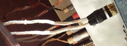
Guys, I completely forgot to insist that you try those wonderful Gold plated OCC copper (6N) wires while they are still on offer. I bought some 20WAG, not only to make some more IC's but also to replace internal wiring inside my amps.
30ft ELF Custom Cables 24k Gold plated Twisted Pair 6N GPOCC Bulk wire 20awg BIN | eBay
I managed to get some more 26AWG also.
As the experts say, once gold goes up, you will not be able to afford it anymore...
Best wishes,
M.
30ft ELF Custom Cables 24k Gold plated Twisted Pair 6N GPOCC Bulk wire 20awg BIN | eBay
I managed to get some more 26AWG also.
As the experts say, once gold goes up, you will not be able to afford it anymore...
Best wishes,
M.
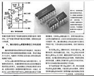
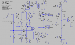
I think it is an idiosyncratic cascoded Kondo shunt regulated push-pull armament.
They are not JFETs and have certainly some kind of dielectric layer. The emphasis was laid on material and thickness.
The 2SK82 and 2SJ28 are vertical power Jfets so no silicon dioxide layer.
They are not JFETs and have certainly some kind of dielectric layer. The emphasis was laid on material and thickness.
Thanks dears.
Indeed, I am finding info online, mainly about the Digital Do Main B-1a amplifier.
http://www.digital-do-main.com/ja/pdf/B-1a_Catalog(English).pdf
I will continue searching for info and sources.
Today I expect to try my new DIY version of the R-VAS.
Good news is that I finally ordered several heatsinks for my future VFETs (TO3) boosttrapped amplifiers and I also bought another set of SONY VFETs at a discount: all to help our friends in HK.
On a totally diferent note, a little bird told me that -ECdesigns- is planning a new version of its DAC.
Best wishes to all,
M.
Thanks so much. I'll take a look.
Report:
The DIY VAS resistor is done. The difference is far from subtle, even while the solder is still hot, so to speak. Briefly, it is like upgrading from a potentiometer to a Transformer based Volume Control (TVC), with improved clarity and definition, and I would say also improved dynamics.
Next time, I will do the frame from PCB thick plastic instead of MDF. If you do not want to buy some expensive low capacitance/low inductance resistors, you can buy some Manganin wire (100 Ohm/m; 1 Ohm/cm) from Conrad and cut one 50cm, or better 2 *1m// sections to wire your own. A star frame was the easiest, or less difficult, to build...
I would like to use those kind of R in all the signal path and see the effect.
Cheers,
M.
Attachments
Hello Max,
The PCB manufacturer is
PCB LAB GmbH
Kettelerstraße 13
72160 Horb am Neckar
Deutschland
Have a look on their Website (unfortunately only in German)
PCB Lab GmbH - Leiterplatten
Here you can find an online calculator and a contact form
Amnesis PCB-Size: 137,7mm x 98,9mm
I gave 2 of my Amnesis PCBs to a good friend who is experienced
in DIY projects. He had problems to equip the PCBs due to the many variants and the close placement of the components esp. of the input stage.
For a rework of the present PCB it should be checked if it is possible
to reduce the number of variants and the number of components a little.
So I will skip the
buffer before the VAS (BC546) because never used
optional current sources proposed by Hans (SMD)
resistors parallel to the 1k resistors of the BS-VAS
Do you still need the CCS-VAS option?
Do you still need all the variants of the BJT input stage
up to 4 transistors feeding the red and yellow LEDs separately
with the bases optionally connected to the top/bottom of the100R resistors.
Are there any wishes from your side concerning the rework.
ECdesigns is often changing their designs, so
I think about ordering one of the present DACs
because it is questionable if the new version
will be available at that low price.
MOS16: up to 96k / 16 bits cost 365 Euros
MOS24: up to 96k / 24 bits cost 700 Euros
Esp. the MOS16 is very inexpensive.
Do you think it is worth spending nearly the double price for 8 bits more.
Best Regards
Would you kindly send me the files for the revised amplifier PCB and the address for the PCB maker?
I will order a bunch and then offer them to the ellect ones.
The PCB manufacturer is
PCB LAB GmbH
Kettelerstraße 13
72160 Horb am Neckar
Deutschland
Have a look on their Website (unfortunately only in German)
PCB Lab GmbH - Leiterplatten
Here you can find an online calculator and a contact form
Amnesis PCB-Size: 137,7mm x 98,9mm
I gave 2 of my Amnesis PCBs to a good friend who is experienced
in DIY projects. He had problems to equip the PCBs due to the many variants and the close placement of the components esp. of the input stage.
For a rework of the present PCB it should be checked if it is possible
to reduce the number of variants and the number of components a little.
So I will skip the
buffer before the VAS (BC546) because never used
optional current sources proposed by Hans (SMD)
resistors parallel to the 1k resistors of the BS-VAS
Do you still need the CCS-VAS option?
Do you still need all the variants of the BJT input stage
up to 4 transistors feeding the red and yellow LEDs separately
with the bases optionally connected to the top/bottom of the100R resistors.
Are there any wishes from your side concerning the rework.
On a totally different note, a little bird told me that -ECdesigns- is planning a new version of its DAC.
ECdesigns is often changing their designs, so
I think about ordering one of the present DACs
because it is questionable if the new version
will be available at that low price.
MOS16: up to 96k / 16 bits cost 365 Euros
MOS24: up to 96k / 24 bits cost 700 Euros
Esp. the MOS16 is very inexpensive.
Do you think it is worth spending nearly the double price for 8 bits more.
Best Regards
Hello Max,
The PCB manufacturer is
PCB LAB GmbH
Kettelerstraße 13
72160 Horb am Neckar
Deutschland
Have a look on their Website (unfortunately only in German)
PCB Lab GmbH - Leiterplatten
Here you can find an online calculator and a contact form
Amnesis PCB-Size: 137,7mm x 98,9mm
Thanks. You're right. I can sing "O sink hernieder,
Nacht der Liebe,
gib Vergessen,
dass ich lebe,
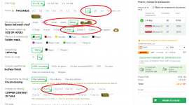
but I cannot order a complex PCB there. I found here publicized a company from Spain that has good price and time response, but I would need advice about technical details, like thickness of the PCB, quantity of copper, minimal size of holes, etc. Please see attached the options.
I gave 2 of my Amnesis PCBs to a good friend who is experienced
in DIY projects. He had problems to equip the PCBs due to the many variants and the close placement of the components esp. of the input stage.
CanI help your friend?
For a rework of the present PCB it should be checked if it is possible
to reduce the number of variants and the number of components a little.
So I will skip the
buffer before the VAS (BC546) because never usedOK. Never got to make it work.
optional current sources proposed by Hans (SMD) OK. Can be fitted on daughter board in case of need.
resistors parallel to the 1k resistors of the BS-VAS.OK. Not needed.
Do you still need the CCS-VAS option?No. That was kept as some asked about them. Don't remember who. I reckon that high quality, non inductive R here would beat active CCS; resistors do not "slew".
Do you still need all the variants of the BJT input stage
up to 4 transistors feeding the red and yellow LEDs separately
with the bases optionally connected to the top/bottom of the100R resistors. We can use daughter-boards IF it is too complicated. The ALLBJT is sounding astonishly good with the DIY VAS resistor. Highly recommended, not to say imperative.
BTW, we can invent other inputs to try. See attachments.
Are there any wishes from your side concerning the rework.
ECdesigns is often changing their designs, so
I think about ordering one of the present DACs
because it is questionable if the new version
will be available at that low price.
MOS16: up to 96k / 16 bits cost 365 Euros
MOS24: up to 96k / 24 bits cost 700 Euros
Esp. the MOS16 is very inexpensive.
Do you think it is worth spending nearly the double price for 8 bits more.
I don't need the extra bits. I was about to buy the 16bit DAC. The new one includes a couple of new inventions that I won't disclose for fear of missrepresent them, but that look very promising.
Best Regards
Attachments
PCB production
Hi Max,
the main problem is if your selected PCB manufacturer can handle
the data output of my layout tool.
I am using a semi-professional tool called TARGET which is popular in Germany/Europe and many PCB manufacturers support the data output of this tool. This tool does not provide Gerber data but uses an own format (file name xxxx.T3001 or older version xxxx.T2001).
You simply send this file to the manufacturer. He knows how to extract
the relevant data for PCB production.
Let me know the web site of the PCB manufacturer in Spain and I hope I can find out if he can handle the TARGET file.
PCB data
thickness usually 1.6mm but 2.4mm is OK too.
size of holes: minimum diameter drill holes is 0.4mm
Space between vias: 8/8 mil 1mil=0.0254mm 8 mil=0.2mm ???
copper content of vias: 2 0z. Cu ??
usually the following parameters are used:
minimum diameter of drill holes e.g. 0.4mm
minimum trace width e.g. 0.2mm
minimum distance e.g 0.2mm
trace to trace
trace to solder pad
solder pad to solder pad
thickness of copper layer usually 35u
The price of 191$ for 20 boards is OK. Does this include shipment costs from Spain to your home town?
Best Regards
Jos,Hi Max,
the main problem is if your selected PCB manufacturer can handle
the data output of my layout tool.
I am using a semi-professional tool called TARGET which is popular in Germany/Europe and many PCB manufacturers support the data output of this tool. This tool does not provide Gerber data but uses an own format (file name xxxx.T3001 or older version xxxx.T2001).
You simply send this file to the manufacturer. He knows how to extract
the relevant data for PCB production.
Let me know the web site of the PCB manufacturer in Spain and I hope I can find out if he can handle the TARGET file.
PCB data
thickness usually 1.6mm but 2.4mm is OK too.
size of holes: minimum diameter drill holes is 0.4mm
Space between vias: 8/8 mil 1mil=0.0254mm 8 mil=0.2mm ???
copper content of vias: 2 0z. Cu ??
usually the following parameters are used:
minimum diameter of drill holes e.g. 0.4mm
minimum trace width e.g. 0.2mm
minimum distance e.g 0.2mm
trace to trace
trace to solder pad
solder pad to solder pad
thickness of copper layer usually 35u
The price of 191$ for 20 boards is OK. Does this include shipment costs from Spain to your home town?
Best Regards
You are wrong.
Target is very well capable of producing Gerber files.
Select:
File - Input/Output Formats - Production - (X-)Gerber and drill output PCBout, or simply press F11 to get there directly.
Hans
- Home
- Amplifiers
- Solid State
- The AMNESIS amp: a good amplifier, like a gentleman, has no memory.