I'd like to warn that the circuit has a fatal failure mode close to clipping due to output VFET cross conduction. Please avoid at all cost.Those are veritable V-FETs (SIT) all right, very valuable, except the Tokin parts that are not in the same class.
Would you take a look at this please:
http://www.amplimos.it/images/hiraga2_Vfet.gif
Hello
In input the stages and the VAS most memory distortion is caused by changes in Vce. Thus a low-gain amp with high input voltage would have more memory than a high-gain amp with low input voltage. One simple way to reduce memory distortion distortion is to use transistors with larger dies, having higher thermal mass, how about ksc3503 or ksc1381 ? I have lot of them, they may need a bit more current from the ccs.
Any thought or ideas about that ?
Thank
Bye
Gaetan
Last edited:
What I meant was both SIT will conduct and self destruct on output close to clipping.Cross conduction is one of many confusedly used notions. ...
Hello
In input the stages and the VAS most memory distortion is caused by changes in Vce. Thus a low-gain amp with high input voltage would have more memory than a high-gain amp with low input voltage. One simple way to reduce memory distortion distortion is to use transistors with larger dies, having higher thermal mass, how about ksc3503 or ksc1381 ? I have lot of them, they may need a bit more current from the ccs.
Any thought or ideas about that ?
Thank
Bye
Gaetan
It should be easy to test. Watch for pinout config.
Bigger mass usually means bigger capacitance, right? Not a good thing...
On the other hand, one could flip over the schematics to use N JFETs as input: Hephaïstos found that KS30 had the best behaviour of all tested devices (30 years ago, it seems) in relation to MD. It has low gain, though...
Cheers,
M.
Two news, one bad and one good:
The bad, one the four channels of Amnesis started oscillating yesterday, as I heard funny "AM radio-like" noises when music stopped, and it got hot. I went back to my 200W light-bulb power cable (the improved DIY cable does clean the picture a lot) and it has behaved today.
I cannot really test it but I will try one or two ideas as soon as the weather improves: coil between amp sections; LEDs instead of Zeners for Vref of the bootstraps.
I believe a two section amp cannot oscillate right?
Mine never did...
That is a good way to try the LTMD input mod. I have been willing to mod my J2 clon but it would be too difficult to dismantle...
The good one is that my 26AWG gold plated OCC copper enamelled wire arrived. I think I can make a 50cm interconnect with it. After listening tests, I will have to decide if a need to double the strands.
I have an appetite for gold these days...
Cheers,
M.
The bad, one the four channels of Amnesis started oscillating yesterday, as I heard funny "AM radio-like" noises when music stopped, and it got hot. I went back to my 200W light-bulb power cable (the improved DIY cable does clean the picture a lot) and it has behaved today.
I cannot really test it but I will try one or two ideas as soon as the weather improves: coil between amp sections; LEDs instead of Zeners for Vref of the bootstraps.
I believe a two section amp cannot oscillate right?
Mine never did...
That is a good way to try the LTMD input mod. I have been willing to mod my J2 clon but it would be too difficult to dismantle...
The good one is that my 26AWG gold plated OCC copper enamelled wire arrived. I think I can make a 50cm interconnect with it.
After listening tests, I will have to decide if a need to double the strands.I have an appetite for gold these days...
Cheers,
M.
I consider everyone in this thread sufficiently warned. I have no need to sacrifice my vfets.... Firstly, keep the rail voltages at a decent level. Have you built the amp according to the schematic diagram?
Last edited:
I consider everyone in this thread sufficiently warned. I have no need to sacrifice my vfets.
Vfets seem to be quite resilient...at least the industrial type should be.
What do you think about a bootstrapped VFET output, like in the SONY TA-N7?
Cheers,
M.
Attachments
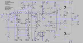
I found more detail explanation by Ilimzn from 2013 on the problem of Hiraga VFET schematic.
With all due respect to Mr. Hiraga, the proposed schematic shows he did not tryly understand how a SIT/VFET works, which is even more surprising considering he was profficient in designing tube (specifically triode) circuits.
DO NOT attempt that schematic as it will not work correctly.
One important thing the schematic is not showing you is that the source terminals of the SIT/VFET are at the output of the amp. Contrary to what Nrik says these parts do NOT need voltages on the agte to conduct, these are depletion mode and with no voltage on the gate (Vgs=0V) will conduct heavily. What they do need is a negative voltage at the gate to STOP them from conducting. The actual voltage that drives then into cut-off deneds on Vds - one more thing where they differ from any other kind of FET. These parts are for all intents and purposes a solid-state triode, and as such ALL of the terminals are inputs. The current Id depends on both Vgs and Vds, with a ratio of mu, a quantity known from triodes as the amplification factor. For 2SK80/2SJ28 this is about 10 on the average (varies with chosen operating point, they are extremely linear at Vds much higher than in the schematic). And this brings us to the problems with the schematic itself.
Mr Hiraga rather unwisely simply transposed his 'darlingnot' circuit which is current driven, into an attempt to make the current of the BJT driver stage into driving voltage for the SIT/VFETs. There are several problems with this:
1) A relatively minor problem is that the required bias voltage for a chosen bias current depends on the power supply voltage. In other words, any sag or ripple will modulate the bias current. The only logical solution that would keep the schematic simple, would be to regulate the power supply.
2) A much bigger problem is what actual bias current the amp will have. There is no means to change it in this simple circuit, and this us really a big problem because the SIT/VFETs have very high tolerances. The 2SK82/2SJ28 available on eBay from acronmanelectronics are actually quite good with this since they all belong to the same 'rank' - VFETs were originally sorted into 'ranks', corresponding to a cut-off voltage. When paralleling or using complements, the idea was to use the same rank in order to get the same characteristics. Acronman sells the same rank for both the P and N part - the rank code is the last digit of the datecode (typically KD33), rank 3. The rank is loosely defined as the Vgs at which Id=100mA at Vds=50V. The encoding is (7.5 + R*2.5)V, where R is the rank number, except for ranks 0 and 1.
Still, this leaves you with the need to adjust various part values in the schematic to get the required bias current. And, with a different pair, it might differ as much as 30% even with the same rank number on the VFETs.
3) MUCH bigger problem, a fundamental one, is a gross mistake in the setup of the circuit which will result in it's destruction when full output is attempted, either voltage or current. Here is why:
If you look at the driver arrangement, the collectors of the driver BJTs are returned to the oposite power supply so that the circuit can give negative gate voltages with respect to the output, where the sources are. But what happens when the output gets close to one of the power supplies? Say, the +V power supply? Well, to do this, the gate of the top VFET is driven more positive, but the gate of the bottom VFET gets less and less 'negative' (with respect to it's polarity) gate drive because there is less and less available negative voltage on the bottom 8.2k resistor. So instead of the top VFET conducting more, and the bottom less, in order to drive the output towards the top rail, the bottom VFET actually starts at some point when the output is approaching the supply rail, to conduct more and more, so current is passed from the + to the - supply. In order for the output to get closer to the rail it requires even more drive which makes the situation even worse, until the circuit latches up. If the heat has not killed it, something else will and that is driving Vgs positive without current limit.
In any case when very high output current is needed, the driver will attempt to connect G to D via it's C-E region. This will drive Vgs positive, into gate current. The problem here is that there is no current limit to the gate drive. The VFET is actually capable of operating in 'enhancement mode' which is actually more like a regular BJT - it exhibits beta (current amplification Ids/Igs, roughly 50 for this type), but the G-S region is a diode and it's absolute maximum current is about 0.5A. For a short circuit on the output (or very low impedance) only the 1 ohm resistor provides a current limit and this may still pass an excessive current through G-S. It will certainly happen in a latch-up condition as mentioned above.
Finally, VFETs are VERY fast. Especially the K82/J28. These were originally used in a class D output stage switching at 0.5MHz, a figure which manufacturers achieve today only within the confines of a single chip, and even then it's a rarity. In the original amplifier that used these parts, the DISCRETE design was able to achieve switching times of about 50nS which is equivalent to output slew rate of 4kV/us. YES they can and often will oscillate without a gate stopper. Add one, it will also limit the gate current.
How to fix this?
1) Regulate the power supply, or provide a means for bias voltage to track the power supply (this would however severely reduce the PSRR figure of the amp so regulation would be a better idea).
2) Provide a means of adjusting the bias voltages. This is not as simple as it requires simultaneous adjustment of two resistors, or an adjustmet of the resistance of a center-tapped balance pot. Also, getting exactly complementary K82/J28 is not easy unless you are willing to do matching amongst a larger contingent. To make things worse, static (DC) and dynamic (AC) balance is not the same thing. A dynamic balance scheme could be incorporated into the schematic, along with the static one already present.
3) Provide floating or bootstrapped power supplies fot he gate drive. Bootstrapping is a must but even in that case having the output stuck close to the rail longer than the bootstrap constant will kill the output stage. Added positive and negative supplies at 2x main supply (aasy to do with voltage doublers and simple regulation) is the right way to go. Provide a means of switching off the main power supply when these are not present (easy to do by providing the reference voltage for the main PSU regulation from these auxilliary power supplies).
4) Add some gate stopper resistors to the gates of the K82/J28. While at it, the 8.2k resistors are really on the high side for driving the input capacitance of the original VFETs specified in the schematic (nearly 1.5nF for the J20! about half that on the K70). K82/J28 are very low capacitance but it's still not trivial. More current through the driver transistors can help.
...and don't try to save money on the heatsink. VFETs are actually extremely robust parts but overheating will kill them. On the plus side, no need to worry about thermal stability, they have negative tempco and in fact for currents over 0.5A it's almost zero.
Ids is determined by the gate to channel voltage. A higher voltage gives a lower current so start out with a low value collector resistor.
To my knowledge, the Sony 2SK60 / 2SJ18 represent the most successful implementation of the concept. I am markedly impressed by both design and technology.
The static induction transistor types in question are in practice unusable as a switch, which is a condition for being outstanding as an audio amplifier.
Whatever the term you find suitable, I'd avoid Hiraga Vfet design and similar fatal design flaw.indra1,
I`m trying to figure out what you mean. We can't call it cross conduction.
Yamaha B2 amp has a complex but interesting way of achieving bias.
Anyway, I prefer SONY's way in the TA-N7, provided my units give good voltages...automatic bias...
Edit: I forgot to mention that both amps are amongst the best amps ever made, if one believes the opinion of the lucky ones that heard both and the present day competition.
The elements that postpone my VFET experiment "à la Sony" are: weather, spare time and suitable L-shaped flank for heat-sink...
I have to mention that my opinion about CLC supply is changing: both amps where I put big DIY chokes (made with common enamelled copper wire, nothing fancy) went from muddy and recessed sound, with soft highs, to "normal" emission in a couple of weeks (intermittent use), retaining ample and deep bass and stage. I am now thinking that it was all due to lack of burn-in. There is certain "liquidity" to the sound, reminiscent of tube amplification.
Cheers,
M.
Anyway, I prefer SONY's way in the TA-N7, provided my units give good voltages...automatic bias...
Edit: I forgot to mention that both amps are amongst the best amps ever made, if one believes the opinion of the lucky ones that heard both and the present day competition.
The elements that postpone my VFET experiment "à la Sony" are: weather, spare time and suitable L-shaped flank for heat-sink...
I have to mention that my opinion about CLC supply is changing: both amps where I put big DIY chokes (made with common enamelled copper wire, nothing fancy) went from muddy and recessed sound, with soft highs, to "normal" emission in a couple of weeks (intermittent use), retaining ample and deep bass and stage.
I am now thinking that it was all due to lack of burn-in. There is certain "liquidity" to the sound, reminiscent of tube amplification.Cheers,
M.
Attachments
Last edited:

Quick update.
I finally built my interconnects with Gold plated OCC copper 26AWG.
The gold plating is very thin obviously. I remember 50um quoted. But the enamel is also very thin and any scratch will peal it, so I had to change my strategy and used only 3 braided wires per polarity and I had to use my cotton sleeve reserve to protect the signal lead.
First impression is very agreeable: full bodied and open sound, even with common connectors; yeah, I ran out of those too.
I am burning-in them before trying them on the big systems.
The good part is that for the reduced introductory price and using 6 strands of 50cm, I will end with 3 pairs of ICs. Not bad for a USD $25 investment...
Apart, I installed 100nF polystyrene caps from source to ground on the VFETs of the SONY TA5650 amp's output. That should help stability. I may have heard an improvement in sound.
Cheers,
M.
I finally built my interconnects with Gold plated OCC copper 26AWG.
The gold plating is very thin obviously. I remember 50um quoted. But the enamel is also very thin and any scratch will peal it, so I had to change my strategy and used only 3 braided wires per polarity and I had to use my cotton sleeve reserve to protect the signal lead.
First impression is very agreeable: full bodied and open sound, even with common connectors; yeah, I ran out of those too.
I am burning-in them before trying them on the big systems.
The good part is that for the reduced introductory price and using 6 strands of 50cm, I will end with 3 pairs of ICs.
Not bad for a USD $25 investment...Apart, I installed 100nF polystyrene caps from source to ground on the VFETs of the SONY TA5650 amp's output. That should help stability. I may have heard an improvement in sound.
Cheers,
M.
50µm is _massively thick_ gold plating, ten times more than "heavily gold plated" connectors. I think you mean 0.50µm plated.
50µm on AWG (radius about 200µm) would mean that 33% of the wire is gold (increasing the average resistivity of the wire somewhat!)
Of course, you are correct. My bad. That's what you get when you write while still sleepy...
Anyway, worth a try.
I crave for gold...what would that be?
Instability is distortion. An amp exhibiting such high instability cannot have good performance.
Are you talking about the SONY TA-5650 which I mentioned?
For some it is one of the best domestic integrated amps ever...
Sony TA-5650 on thevintageknob.org
Cheers,
M.
- Home
- Amplifiers
- Solid State
- The AMNESIS amp: a good amplifier, like a gentleman, has no memory.