Now listening to the JFETinput-MPSA18 VAS with an AK4393 based DAC with discrete LTMD differential amplifier output: it sounds as if there was a magnifying glass
Edit: he doesn't forgive bad recordings though...
The "Ultimate NOS DAC..." thread was inaugurated 12th May 2006, 04:07 PM! John went through several iterations until he gave up on the TDA1541 chip and decided to create his own converter. I could quote him but I prefer not to send unrequested infoYou should give it a try. Look, now that you mention "reviews" I did a quick search and found one review from a former version (previous to mine) of the DAC (the guy is an extreme perfectionist), and several conversation on different fora:
EC Designs Mosaic T DAC | HFA - The Independent Source for Audio Equipment Reviews
I'll stop propaganda now.
Cheers,
M.
I'm just glad you are completely happy with your gear, enjoy it as much as you can.
What exactly does LTMD stand for, perhaps Low Thermal Distortion?
You made me a bit curious on the new EC Dac. A Dac is a Nos Dac or it isn't, there is nothing in between.
So it could possibly be a DSD type of converter, converting in the MHz region and having no DAC at all or one with only a few bits.
Do you have any more info, or should I contact EC for that ?
I can't find anything on the Web.
Hans
Sorry. Yes. it stands for Low Thermal Memory Distortion just to denote the input configuration for the diff amp, not to imply any real life effect, hehe. In that particular circuit it was a compound CFP (JFET to BJT) bootstrapped with a JFET.
That dozen year old digital thread, now devoted to a simultaneous mode TDA1541A DAC, produced for me two decent DACs based on the obsolete TDA1543, one of which is on "Tape sound" realm, but measures awfully, I'm sure. And yes, it mates wonderfully with the Amnesis, as you so rightfully predicted. (awful picture attached)
Building the ultimate NOS DAC using TDA1541A
About the Mosaic, there are a couple of extensive posts there where John Brown describes in detailed mode the whole, but, obviously, now I cannot find them, so I will paste short (and old) quotes from him, just for you to have an idea. It is better that you write (or phone) to him as I am sure he will be glad to converse with you about the myriad of technical problems he had to solve.
For example, about I2S, he managed to silence signals for the unused 75% of the time of a 16bit DATA on 64bit frame...or something to that effect...for a more silent background.
I hope this helps,
M.
That dozen year old digital thread, now devoted to a simultaneous mode TDA1541A DAC, produced for me two decent DACs based on the obsolete TDA1543, one of which is on "Tape sound" realm, but measures awfully, I'm sure.
And yes, it mates wonderfully with the Amnesis, as you so rightfully predicted. (awful picture attached)Building the ultimate NOS DAC using TDA1541A
About the Mosaic, there are a couple of extensive posts there where John Brown describes in detailed mode the whole, but, obviously, now I cannot find them, so I will paste short (and old) quotes from him, just for you to have an idea. It is better that you write (or phone) to him as I am sure he will be glad to converse with you about the myriad of technical problems he had to solve.
For example, about I2S, he managed to silence signals for the unused 75% of the time of a 16bit DATA on 64bit frame...or something to that effect...for a more silent background.
It’s not a (segmented) R2R ladder DAC like the PCM1704 or the Soekris DAC for example.
The Mosaic D/A converter core can best be described as a discrete common-rail matrix DAC and it runs on a multi-stream interface, not I2S.
Decoder is required for translating I2S into multi-stream. This is a discrete state machine decoder that runs on a +/- 0.8V balanced power supply. The decoder is specifically designed to offer very high speed and very low switching noise.
The multi stream interface contains multiple serial data signals, serial rail control signals and timing signals.
The Mosaic D/A converter only contains logic circuits and a resistor matrix. The balanced power supply offers DC-coupled output (4Vpp, 200 Ohm output impedance).
Report Post Reply With Quote
The multi stream interface contains multiple serial data signals, serial rail control signals and timing signals.
The Mosaic D/A converter only contains logic circuits and a resistor matrix. The balanced power supply offers DC-coupled output (4Vpp, 200 Ohm output impedance).
I use 7400 series bus storage registers for the Mosaic UV and 7400 bus storage registers and 7400 series octal D flip-flops for the Mosaic II. These are similar devices as used in most discrete R2R ladder DACs.
We have to face the fact that there are no perfect components, ok we might get parts with say 1 Ohm RDSon but these will cause new problems (higher surge currents, higher ground-bounce, more pollution) especially with the given parasitics of a relatively large discrete circuit.
The same imperfect devices can be used in different ways to improve performance. The Mosaic converter circuit -looks- similar to conventional discrete R2R ladder DAC circuits, except, it is no R2R ladder DAC.
Most popular discrete R2R ladder DACs are based on simple voltage attenuators based on two resistors (R and 2R).
For higher precision Wheatstone bridges are used.
That's what I used for the Mosaic matrix converter and that's why accuracy is no longer an issue.
The remaining small bit errors are below the audibility threshold. These errors can be easily nulled by trimming.
The Mosaic UV DAC has no output buffer (passive output). There are fixed outputs (750 Ohms) and a variable outputs (0 - 5K).
Ternary logic switches switch between -2V8, 0V and +2V8. This logic drives a passive resistor matrix that has 750 Ohms output impedance. The output is DC-coupled since it swings symmetrically around GND, so no coupling caps in the signal path either.
The +2V8 is provided by a discrete quatrode voltage regulator, the tracking -2V8 is derived from a second discrete quatrode regulator and a servo circuit that compares both plus and minus voltages and corrects the negative voltage for tracking. This way there is no DC on the outputs.
I hope this helps,
M.
Attachments
Last edited:
Hi Max,Sorry. Yes. it stands for Low Thermal Memory Distortion just to denote the input configuration for the diff amp, not to imply any real life effect, hehe. In that particular circuit it was a compound CFP (JFET to BJT) bootstrapped with a JFET.
That dozen year old digital thread, now devoted to a simultaneous mode TDA1541A DAC, produced for me two decent DACs based on the obsolete TDA1543, one of which is on "Tape sound" realm, but measures awfully, I'm sure.
Building the ultimate NOS DAC using TDA1541A
About the Mosaic, there are a couple of extensive posts there where John Brown describes in detailed mode the whole, but, obviously, now I cannot find them, so I will paste short (and old) quotes from him, just for you to have an idea. It is better that you write (or phone) to him as I am sure he will be glad to converse with you about the myriad of technical problems he had to solve.
For example, about I2S, he managed to silence signals for the unused 75% of the time of a 16bit DATA on 64bit frame...or something to that effect...for a more silent background.
I hope this helps,
M.
Thanks a lot,
You know what, I'll dive into the original 2006 thread and try to read it from start to end.
One thing puzzles me: The 16 bit Dac he is currently offering is a steal at 363,- Euro's and the 24 bit top version only 695,-.
And I believe your judgement that they sound very good.
Why isn't he successful into getting more attention to his product.
The well known top dac's are still very expensive ??
Hans
Hi Max,
Thanks a lot,
You know what, I'll dive into the original 2006 thread and try to read it from start to end.
Oh! That is very brave but I am exhausted only to think of it. Mind you, the first several years were invested in the development of "direct-interpolation" multi DAC chip DACs, which were then abandoned, meanwhile encountering and solving dozens of real life problems of digital realm, which is analog at the end... then after all this titanic journey, he decided to start from scratch: you would benefit much more if you perhaps tried to appoint a visit with listening session...just saying.
One thing puzzles me: The 16 bit Dac he is currently offering is a steal at 363,- Euro's and the 24 bit top version only 695,-.
Indeed! The MOS16 costs a fourth of the MOSAIC UV, which was payed with my last (and I do mean my last) tax refund
This a sign of the dawning of Aquarius era: altruism as a reasonable way of interaction
And I believe your judgement that they sound very good.
As one mate's signature here says: "the test of the machine is in the satisfaction that it gives". Your body will know if it is "good enough".
Why isn't he successful into getting more attention to his product.
Several reasons come to mind...He probably relies on mouth to mouth spread...he is comfortable with the state of affairs and does not want to grow...besides it is known that inventors (and real philosophers) are payed-off, are satisfied with the knowing and the achievement itself and seldom are good businessmen...
The well known top dac's are still very expensive ??
Hans

I confess Toslink still worries me...the remnants of a past audiophile life...
BTW, with the Amnesis output, apart from VFETs which are very expensive, perhaps Depletion Mode MOSFETs (less expensive?) can be found and simulated for an "automatic biasing" Bootstrap which would save us lots of parts. Not because these parts are expensive but because every redundant subcircuit has the potential to jeopardize stability. I trust my VFETs will auto-bias at +/-12V more or less.
Cheers,
M.
Last edited:
Allow me to hyjack my own thread.
Dear all,
For those who are thinking, why is this guy always talking about the VFET bootstrapped output??? Perhaps you never had the joy of listening to a VFET amp... VFETs have a delicacy, a crystalline quality, much like tubes, which cannot be equaled by other output devices, IMHO.
I have the luck to own three of these amps, one of which is a glory of the golden age of Japanese electronics, namely the SONY TA-5650 amp which I bought for pennies as a non functioning unit. My gamble succeeded as all the 8 VFETs were good, and after much repairing and modifying I finally tested it: one channel good; the other, oscillating.
I then tried all the advices published on the net (safe one, I confess) to no effect.
Then I postulated that the common-source arrangement (predriver-driver-output) as it was, could be forming a Colpitz with the capacitance of the bigger and slower VFETs being the culprit. So I decide to try and cascode the output (yeah, I know I am mono-maniac) to bring the resonant freq. much upwards...it worked.
Now I am considering improving or changing the output, as I have some MOSFETs, but being a coward as I am with this jewel, I will again abuse of your generosity by posting here the present stage of the amp to seek your advice and comments.
Questions:
1) is my diode string redundant, from a bias POV? In other words, will the voltage on the emitter set itself with the biasing pot as it is? Since the current is set by the common-source VFETs...
Now the Vce is under 8V, for these low SOA transistors, which BTW, are the same the flagship TA-N7 uses, though in common-collector arrangement.
2) if I swap the output BJTs for the MOSFETs IRFP9240/240, will their sources set themselves to a +4V and -4V, respectively, compared to their gates???
This question is related obviously to the former and makes evident my lack of basic knowledge...only empiric I have...
I understand I can reference the pots to output instead of ground, to form a true bootstrap, like in the case of the Amnesis, at an increased risk of oscillation...talking about which, I must mention that the other potential cause of oscillation which I must address is the one caused by the zobel injecting HF into ground and then transmitting it to the input, on a susceptible layout, like this one, pre-software era, seems to be. In this case it is recommended that the R-C zobel, be connected after the output R//coil, in case of said oscillation.
This was the most demanding project (even bigger than the Amnesis) so far, due to the fact that repairing and debugging is much more difficult than building...my deepest respect to technicians who have to deal with these problems.
I hope you like my crazy story and thanks in advance.
Cheers,
M.
PS: I forgot to mention that it has the "first generation" LTMD input mod. No space for more complex mods...though I must cascode the input CCS at some point.
Dear all,
For those who are thinking, why is this guy always talking about the VFET bootstrapped output??? Perhaps you never had the joy of listening to a VFET amp...
VFETs have a delicacy, a crystalline quality, much like tubes, which cannot be equaled by other output devices, IMHO.I have the luck to own three of these amps, one of which is a glory of the golden age of Japanese electronics, namely the SONY TA-5650 amp which I bought for pennies as a non functioning unit. My gamble succeeded as all the 8 VFETs were good, and after much repairing and modifying I finally tested it: one channel good; the other, oscillating.
I then tried all the advices published on the net (safe one, I confess) to no effect.
Then I postulated that the common-source arrangement (predriver-driver-output) as it was, could be forming a Colpitz with the capacitance of the bigger and slower VFETs being the culprit. So I decide to try and cascode the output (yeah, I know I am mono-maniac) to bring the resonant freq. much upwards...it worked.
Now I am considering improving or changing the output, as I have some MOSFETs, but being a coward as I am with this jewel, I will again abuse of your generosity by posting here the present stage of the amp to seek your advice and comments.
Questions:
1) is my diode string redundant, from a bias POV? In other words, will the voltage on the emitter set itself with the biasing pot as it is? Since the current is set by the common-source VFETs...
Now the Vce is under 8V, for these low SOA transistors, which BTW, are the same the flagship TA-N7 uses, though in common-collector arrangement.
2) if I swap the output BJTs for the MOSFETs IRFP9240/240, will their sources set themselves to a +4V and -4V, respectively, compared to their gates???
This question is related obviously to the former and makes evident my lack of basic knowledge...only empiric I have...
I understand I can reference the pots to output instead of ground, to form a true bootstrap, like in the case of the Amnesis, at an increased risk of oscillation...talking about which, I must mention that the other potential cause of oscillation which I must address is the one caused by the zobel injecting HF into ground and then transmitting it to the input, on a susceptible layout, like this one, pre-software era, seems to be. In this case it is recommended that the R-C zobel, be connected after the output R//coil, in case of said oscillation.
This was the most demanding project (even bigger than the Amnesis) so far, due to the fact that repairing and debugging is much more difficult than building...my deepest respect to technicians
who have to deal with these problems.I hope you like my crazy story
and thanks in advance.Cheers,
M.
PS: I forgot to mention that it has the "first generation" LTMD input mod. No space for more complex mods...though I must cascode the input CCS at some point.
Attachments
Last edited:
Maybe you will find SissySIT thread interesting. Zen Mod makes a Vfet power amp with a Tokin VFET in Pass forum where we prefer simpler circuit.... why is this guy always talking about the VFET bootstrapped output??? Perhaps you never had the joy of listening to a VFET amp...
Max,Questions:
1) is my diode string redundant, from a bias POV? In other words, will the voltage on the emitter set itself with the biasing pot as it is? Since the current is set by the common-source VFETs...
Now the Vce is under 8V, for these low SOA transistors, which BTW, are the same the flagship TA-N7 uses, though in common-collector arrangement.
2) if I swap the output BJTs for the MOSFETs IRFP9240/240, will their sources set themselves to a +4V and -4V, respectively, compared to their gates???
This question is related obviously to the former and makes evident my lack of basic knowledge...only empiric I have...
3) I understand I can reference the pots to output instead of ground, to form a true bootstrap, like in the case of the Amnesis, at an increased risk of oscillation.
4) I must mention that the other potential cause of oscillation which I must address is the one caused by the zobel injecting HF into ground and then transmitting it to the input, on a susceptible layout, like this one, pre-software era, seems to be. In this case it is recommended that the R-C zobel, be connected after the output R//coil, in case of said oscillation.
Let me try to answer in the best possible way starting with:
3) The pots Must be referenced to the output, or else the BJT will be shut off above Vout>+/- 6.5 Volt, but it seems as if there was a second pair of Vfets that you removed , why was that ?
And why did you insert the two BJT's where now all current has to flow through, BJT's who aren't suited for the job with only 10 Watt each.
2) Replacing these BJT's by Mosfets can be done, gates to the output signal, because the Vfets determine the amount of current that will run, so they Mosfet's will bias themselves to this current.
1) I do not understand your question, but I also don't get why you are inserting BJT's or Mosfets in the first place. The original Vfets are supposed to do the job of driving the output.
4) It is very important to have the feedback signal properly routed, preventing to pick up other signals from within. Sometimes a wire in the air will help.
Also very important is the point where the feedback signal starts, This should be taken from the final line going to the Amp's output.
As for the grounding, this comes also very critical to keep the signal gnd at the input as clean as possible, but much has been published about the subject.
When everything is well done, I don't see how a Zobel network may reduce stability.
5) The other thing that strikes me is that this amp has no Miller Cap, possibly making it more difficult to get the amp stable.
Hans
Thanks, dear Hans, for your help.
Thanks, dear Indra1,
Cheers,
M.
Max,
Let me try to answer in the best possible way starting with:
3) The pots Must be referenced to the output, or else the BJT will be shut off above Vout>+/- 6.5 Volt, but it seems as if there was a second pair of Vfets that you removed , why was that ?
And why did you insert the two BJT's where now all current has to flow through, BJT's who aren't suited for the job with only 10 Watt each.
OK. That move, pot-to-output, is easily done.
Maybe I don't see the clipping because I drive the amp very gently...
As I tried to explain, inserting the BJT in common-base was intended to reduce Miller (and Early?) effect...I chose these low power devices to be a life-guard to the VFEts: they shall blow before the former in case of malfunction, or that was my idea. The next move was supposed to be higher power BJT (or MOSFETs) with the pot biased at, lets say +/-35, to reduce VFETs' Vds...but I never reached that stage of the plan: the Amnesis was the priority; every time I mod this beautiful amp, I suffer
For example, yesterday I opened it and answered my own question
Oh, and I am using now only 4 VFETs: that way only 4 are at risk; I have 4 extra VFETs for other projects
2) Replacing these BJT's by Mosfets can be done, gates to the output signal, because the Vfets determine the amount of current that will run, so they Mosfet's will bias themselves to this current.
Thanks!
That's what I thought but was too coward to test it.
1) I do not understand your question, but I also don't get why you are inserting BJT's or Mosfets in the first place. The original Vfets are supposed to do the job of driving the output.
As I tried to explain, my thought was that the triple with common-emitter output has feedback that can form a Colpitts oscillator, with the capacitance of the VFET, the bigger unit, being the offender. So by reducing that capacitance the resonance point will be shifted upwards. Am I right?
BTW, I have the intuition that these common-emitter/common-source output amps sound inherently better than the common-collector/common-drain ones...but are much difficult to design.
4) It is very important to have the feedback signal properly routed, preventing to pick up other signals from within. Sometimes a wire in the air will help.
Also very important is the point where the feedback signal starts, This should be taken from the final line going to the Amp's output.
The FB is properly taken, IMHO.
As for the grounding, this comes also very critical to keep the signal gnd at the input as clean as possible, but much has been published about the subject.
When everything is well done, I don't see how a Zobel network may reduce stability.
It is my understanding that the zobel can inject HF noise into the "ground" and if that this "ground" is not properly routed, as seems to be the case here (I won't post the PCB not to overload you) it can contaminate the input...
5) The other thing that strikes me is that this amp has no Miller Cap, possibly making it more difficult to get the amp stable.
I am inclined to believe that it now does...
Hans

Thanks, dear Indra1,
Maybe you will find SissySIT thread interesting. Zen Mod makes a Vfet power amp with a Tokin VFET in Pass forum where we prefer simpler circuit.
I do follow that thread, but more for ZM comments
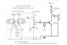
I have great results with summing my LTMD differential input section to my single ended class A Tokin SK180 amp.
I have all the needed parts (safe PSs) to make another, bigger, amp with this configuration but with THF51 TOKINs. When I finally make it will post it and you will see the size of the box!
In other words: only "Low Thermal Memory Distortion" amps for me, thank you...whatever that means
Which reminds me: I shall be posting used and unused amplifiers for sale on the trading section...
Cheers,
M.
Attachments
Last edited:
O.K., now I understand what you were aiming at, reducing the effect of the Cgd of the Vfet.
However, the gate from this Vfet is driven from a very low resistance with a low voltage swing, so I have no idea whether this will sort any effect, other than adding an extra pole in the equation. Often less is more.
But with enough phase margin will it be possible to add a BJT or Mosfet in the Vfet's drain, but in that case with a much higher fixed voltage for the base (or the gate) , like 40 volt, and not be tied to the output in that case.
With this marginal BJT that you have now, you can't do that, you will need a real power device.
And with the protection circuit installed, I see no reason why you should be afraid of frying a VFet. You can even set the tripping points a bit sharper to start with.
And always put something in series with the PSU when switching the Amp on after a mod. This can very well be a 12Volt car bulb, at the same time serving as fuse and as the lighting prove that current consumption is under control..
It will be a matter of trial and error and a lot of listening.
About the Zobel network, no problem to send me pictures taken from the PCB.
Hans
O.K., now I understand what you were aiming at, reducing the effect of the Cgd of the Vfet.
However, the gate from this Vfet is driven from a very low resistance with a low voltage swing, so I have no idea whether this will sort any effect, other than adding an extra pole in the equation. Often less is more.
But with enough phase margin will it be possible to add a BJT or Mosfet in the Vfet's drain, but in that case with a much higher fixed voltage for the base (or the gate) , like 40 volt, and not be tied to the output in that case.
With this marginal BJT that you have now, you can't do that, you will need a real power device.
And with the protection circuit installed, I see no reason why you should be afraid of frying a VFet. You can even set the tripping points a bit sharper to start with.
And always put something in series with the PSU when switching the Amp on after a mod. This can very well be a 12Volt car bulb, at the same time serving as fuse and as the lighting prove that current consumption is under control..
It will be a matter of trial and error and a lot of listening.
About the Zobel network, no problem to send me pictures taken from the PCB.
Hans
Thanks Hans,
Much appreciated. These old amps are delicious, and more so with my mods
I recommend to whomever crosses with one of these, consider purchase...
Sony TA-5650 on thevintageknob.org
In Europe it can also be found as Wega V-4810, as stated on the link.
I understand and had previewed what you explained about the power output devices and biasing. I am learning after all. Something alike what we did for the cascoded VAS of the Amnesis. As I understand from what you mentioned, in that case it should be a true cascode, with pot-to-ground, instead of a bootstrap, with pot-to-output...my plan is as follows: use the unused spots on the heatsink for my canned MJE15024/25 to be used as a cascode for the VFETs. More elegant. Now that I proved that the units are stable with the little cascodes, I can go further and delete those horrible daughter boards that I am using. I can connect a Zener (6,1V-8,2V to give the VFETs a little air) from PS to base and then a 2K-3K resistor from base to ground. I did not catch why I cannot tie it to output instead...
I will try to simulate such an amp, with MOSFET instead of VFET to try to see what happens...About the protection circuit, obviously in stock form it failed to protect because these amps are famous for failing and killing the outputs: it is said that the varactors (VD-1221) AKA "suicide diodes", used to set bias current, used to become shorted...possibly so...but it is maybe due to the fact that the amp is prone to oscillation; for example some reported that with tone control to max. HF some units oscillate. I disabled that board.
I remember I did some recommended mods in that protection circuit. I will try to understand how it works and see if I already did some mod...maybe that is why the 0R33 output (drain) resistors are there instead of being used as source degeneration resistors?
Anyway, not only now I have a stable amp but also, as you probably suspect by now
, I am partial to the sound of cascoded outputs and I think it sounds better this way...Cheers,
M.
PS: at some point I added Miller compensation but then I took it out, apparently...
PS2: for mods, I use 100Watt light bulbs. Smaller ones could make the critical voltages go too down and derange everything and "pumping" or "motor boating".
Last edited:
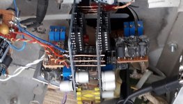
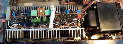
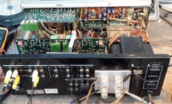
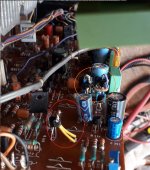
Here, some pics about the present state of the SONY TA-5650, while I rest and plan the next move.
I recorded a video with my portable phone but it does not sound good...I will try to make something better...
Cheers,
M.
PS: I forgot I opened an exclusive thread for this but failed to update it...
I recorded a video with my portable phone but it does not sound good...I will try to make something better...
Cheers,
M.
PS: I forgot I opened an exclusive thread for this but failed to update it...
Attachments
Hi Max,Here, some pics about the present state of the SONY TA-5650, while I rest and plan the next move.
I recorded a video with my portable phone but it does not sound good...I will try to make something better...
Cheers,
M.
PS: I forgot I opened an exclusive thread for this but failed to update it...
What you've done makes no sense.
When wanting to reduce the miller effect of the Vfet's, the drain should be kept at a fixed voltage, which is only the case when the external pots are connected to gnd.
In the current set up the drain moves with the same voltage swing as the output, only reducing the power consumption in the Vfet's a bit, but that is most likely not necessary.
So first try to let the thing work without the added BJT's in the output stage until you are happy with the sound.
At a later stage you can always extend your experiments.
Hans
Hi Max,
What you've done makes no sense.
When wanting to reduce the miller effect of the Vfet's, the drain should be kept at a fixed voltage, which is only the case when the external pots are connected to gnd.
In the current set up the drain moves with the same voltage swing as the output, only reducing the power consumption in the Vfet's a bit, but that is most likely not necessary.
So first try to let the thing work without the added BJT's in the output stage until you are happy with the sound.
At a later stage you can always extend your experiments.
Hans
Maybe,
I've tried it both ways and now I am doing listening tests. It does not sound bad at all. When I'll upgrade to big power BJTs, I'll tie them to ground, as you recommended.As I see it, now the BJTs are fed with signal from two pins.
In a perfect world, I would attach a switch to swap from one to the other option and try to discriminate if the "sensical" option outperforms the "wrong" one
We can explore options based on an hypothesis from the accepted model but sometimes we could find unexpected results...that makes experimentation fun. Or, we can be totally fulled by our own expectations.
Thanks!
M.
Hi Max,
I agree with Hans, I'm not sure where you are going with this circuit.
If Connect the 10K pots to ground and not to the outout as shown, then
the BJTs will cascode the VFets, but it will limit output to +/- 10volts.
I observe the cascode BJT's are only rated at 10W each and have a Vceo
of 30volts so youc can't increase the voltage very much, perhaps 14V as a
reasonable max voltage or the BJTs will self destruct near clipping.
As Shown the BJT's are operating within safe limits, apart from running in
parallel without current sharing emitter resistors isn't a reliable way to
double power handling.
Anyway, an interesting experiment, just watch the limitations of the
devices.
Regards,
Symon
Guys, thanks for manifesting your concerns. I always learn from your advices. 
I know about current sharing.
The listening tests are performed in the Tannoy Autograph clone system: Beyma coaxials are 98db/W/m for the woofers, plus the amplifying effect of the front and back loaded horns.
I am confident that the amp is working in the milliwatt region most of the time.
Check out my signature later. I will post a short video (recorded with my phone) of a TV video from the 70's I downloaded from youtube. That way they cannot block it.
I assume it is videotape transfered to digital: ADD.
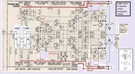
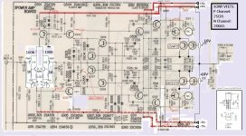
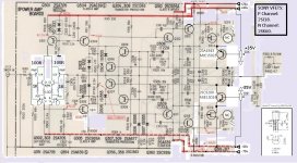
Attached is the future plan for the Sony. I am exploring a "common-source Amnesis" project also, just for fun.
Chhers,
M.
I know about current sharing.
The listening tests are performed in the Tannoy Autograph clone system: Beyma coaxials are 98db/W/m for the woofers, plus the amplifying effect of the front and back loaded horns.
I am confident that the amp is working in the milliwatt region most of the time.
Check out my signature later. I will post a short video (recorded with my phone) of a TV video from the 70's I downloaded from youtube. That way they cannot block it.
I assume it is videotape transfered to digital: ADD.
Attached is the future plan for the Sony. I am exploring a "common-source Amnesis" project
also, just for fun.Chhers,
M.
Attachments
Last edited:
That looks much better.Guys, thanks for manifesting your concerns. I always learn from your advices.
I know about current sharing.
The listening tests are performed in the Tannoy Autograph clone system: Beyma coaxials are 98db/W/m for the woofers, plus the amplifying effect of the front and back loaded horns.
I am confident that the amp is working in the milliwatt region most of the time.
Check out my signature later. I will post a short video (recorded with my phone) of a TV video from the 70's I downloaded from youtube. That way they cannot block it.
I assume it is videotape transfered to digital: ADD.
Attached is the future plan for the Sony. I am exploring a "common-source Amnesis" project
Chhers,
M.
The BJT's will draw quite some base current, so it may be wise to also put caps to gnd.
Isn't this a fantastic hobby ?
I'm anxious to hearing your listening experience.
Succes, Hans
That looks much better.
The BJT's will draw quite some base current, so it may be wise to also put caps to gnd.
Isn't this a fantastic hobby ?
I'm anxious to hearing your listening experience.
Succes, Hans
Thanks!
I updated my signature. Of course, the phone's mic does not make it justice.
I will post more short clips, but I have no patience to edit the circumstances.
This is the pre+power connected: big spades from speaker cables did not allow direct power amp connection from TVC. I have to get rid of those, as I prefer bare cable.
Amadeus Quartet playing Beethoven's (I think) 6th string Q live on TV.
Yeah, I will use the pot just to find optimal operation point and then maybe zener//cap to PS with a big 1K to 2K resistor to ground...and then swapping to output?
I have to see what is better, if cap to PS or cap to ground. Potential difference will be smaller from base to PS...
I have to see what is better, if cap to PS or cap to ground. Potential difference will be smaller from base to PS...
You’re right
Hi Max,
minor point, but the objective of the BJT's is to keep the voltage across the FETs
constant to reduce capacitive effects. So the BJT reference should be the power rail.
That way it eliminates power rail noise or sag from affecting the FET.
I think this makes life easier as you just need a 10Volt zener and capacitor from
each of the power rails to set the respective BJT base voltage.
Also the MJ15024/5 devices are rather slow FT 4Mhz and low gain 15 to 60 compared
to the 2SC5200 / 2SA1941 pair (FT 30Mhz and gain of 75 to 150). So you need to
pick bias current carefully depending on which you use.
Regards,
Symon
- Home
- Amplifiers
- Solid State
- The AMNESIS amp: a good amplifier, like a gentleman, has no memory.