Input stage
I tested successfully the proposal from Hans (post #475 using only BC5xx transistors) with my test amp.
@ Hans: Why do use 3 LEDs for D1/D2. Simulation shows the same result for THD when using only one LED.
Beneath providing solder pads for connecting a daughter board I'm looking to find AllBJT versions that can be placed on the main board.
One candidate is the proposal from Hans. Max do you have another proposal which is not too complex.
Output stage
Emitter resistors R9/R12 are 0.3 Ohm for simulation.
Can I use 0.22 Ohm or better 0.33 Ohm for real amp?
The optimal quiescent current (125mA) will be measured as voltage drop across R9 or R11??
Depends the optimal quiescent current from the used resistor value
(0.3/0.22/0.33 Ohm)??
Cheers
Hi Jos,
The reason for using more Leds is to increase Vce on the input transistors, thereby decreasing the capacitances of these transistors.
This has a direct positive effect on stability.
A second effect is that thermal distortion, one of the main issues here, will be reduced by a factor 3 to 4 when the current flowing through the input transistors is varying by a certain amount
And yet another positive side effect is that Vce on the two PNP's will be reduced to ca 36 Volt when using a 44 Volt supply.
Most BCxx transistors can only have 40 Volt, so this is a potentially critical spot for a transistor.
As for the emitter output resistance value, the lower the better as far as linearity concerns. However, thermal stability becomes more and more an issue when lowering this resistance value.
I would say that 0.22 Ohm as an optimum is better as a 0.33 Ohm, still with the 125mA quiescent current.
Hans
See answers inside .
I will also try to comment in the critical VAS transistor.")
Thanks guys.
M.
Input stage
I'm working on a combined layout for the JFET and AllBJT input stage.
There exist several versions for the AllBJT input which are more or less complex. It's not possible to cover all the versions on the main board. The complex versions which are not perfect yet and subject to change must be shifted to a daughter board.
OK. Just put enough holes for optional connections.
I tested successfully the proposal from Hans (post #475 using only BC5xx transistors) with my test amp.
@ Hans: Why do use 3 LEDs for D1/D2. Simulation shows the same result for THD when using only one LED.
We use several LED/diodes to achieve desired operational points in simulation. Choosing different LEDs cause different outcomes IN SIMULATION. Since I cannot predict operational points, I try them all and see what works, in simulation. IN REAL LIFE two (2) yellow LEDs give me 3,5V and 1 (one) red LED gives me 1,5V to set operational points for the bases of the different cascodes and bootstraps. Since there are many LED color options which give different voltage drops, one can try optimal values from TMD, THD and stability POW, as Hans commented. A variable resistor is also useful to set the optimal operational points, but I think, at a probably increased risk of oscillation, perhaps.
So, where simulated schematics show three (3) LEDs/diodes, in reality two (2) LEDs will be enough.
The latest proposal from Max/Symon (post #488) differs completely from proposal (post #476).
@Max: Is proposal (post #488) your favorite now.
Simulations show that the voltage drop across the LED/Diodes is
very critical for the functionality.
When increasing the voltage drop D16/D11/D13 to increase Uce for Q11/Q12 the simulation does not work.
Is it advising to use LED LXK2-PW14 which is a power LED (Vf=3.6V @350mA) for simulation.
As stated before, I used that LED for convenience as it gave me good simulations. In reality two yellow LEDs will work OK.
Which components did you use for D9 and D16/D11/D13 in your test amp for listening tests (the LEDs used for simulation are not suited for a real amp or hard to order).
Common diodes, I believe are 1N4148-7. Nothing fancy.
Beneath providing solder pads for connecting a daughter board I'm looking to find AllBJT versions that can be placed on the main board.
One candidate is the proposal from Hans. Max do you have another proposal which is not too complex.
ALLBJT versions shall need at minimum one extra transistor for each bootstrapped pair (two BJT minimum) one extra resistor for each CCS (4 resistors) and one or two LEDs for each bootstrapped BJT (6 LEDs). I will provide schematics later.
Output stage
Emitter resistors R9/R12 are 0.3 Ohm for simulation.
Can I use 0.22 Ohm or better 0.33 Ohm for real amp?
The optimal quiescent current (125mA) will be measured as voltage drop across R9 or R11??
Depends the optimal quiescent current from the used resistor value
(0.3/0.22/0.33 Ohm)??
Cheers
I will also try to comment in the critical VAS transistor.
Thanks guys.
M.
Last edited:
Guys, tomorrow we commemorate the first anniversary of this mighty project
and I have to go to the lake for a week, probably without easy internet access, so...
Just in case I wasn't very clear, I use 5mm common type LEDs as I bought a bunch of them on eBay for some pennies. I now realize that JOSI1 was asking about these sorry for the wrong previous answer.
VAS cascode LEDs must be 5mm diameter: two yellow or amber yellow worked always without problems. IF you find a blue one that gives you 3.6 to 4V in real life, good for you.
Setting operation points for ALLBJT:
One way is replacing the active subcircuits with a V source and doing simulations to find preferred voltages and currents. Then finding the right LED combination that gives you the desired points. As I said, for me is as follows...
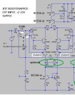
LED for CFP's internal cascode (sorry I don't use numbers here as they might change in different diagrams) which I refer as RED LED (but can be any color that gives you the right V reference point) is a 2mm diameter (tinny) LED as this one passes little current.
LEDs for the main bootstrap BJT (external to the CFP) two yellow (or other color) LED that gives you at least 3.5V drop. Here I used my Chinese 5mm diameter ones but I believe that 2mm diameter ones can also be used to save some area...
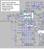
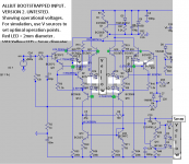
I attach some diagrams for the JFET bootstrapped input (tested with 32V supplies), for the ALLBJT version 1, which is what I am using now and for ALLBJT version 2 untested with 4 extra BJTs for active bootstrapping. Those might be reduced to 2 BJTs. I mark possible connection points for daughterboards with green stars.
Now for the VAS BJT, I managed to use successfully MPSA18, this time with an increased value of 10R for the emitter degeneration resistor (instead 3R) which I forgot to do last time, and with 130R gate stopper resistors for the MOSFETs. With the recommended "charge-transfer" linear supply I do not detect bursts of oscillation.
Again, both transistors, BD139 and MPSA18, have IMHO different behaviors. I would say the former is "darker" sounding, with lots of weight and punch and makes my 35W amp sound like a 400W amp, a feature that dear JRZoid should welcome. The MPSA is more refined and ethereal, more focused and detailed. But now I do not sense a "hole" in the midrange as before, which was due, most probably, to oscillation outside the reach of my humble oscilloscope.
It is early so my opinion on sound could change. Anyway, "transistor swapping" (to make the parallel with tubes) is encouraged in this position.
I expect 2N2222 to arrive. I hope they will be good.
Best wishes for you all.
M.
and I have to go to the lake for a week, probably without easy internet access, so...
Just in case I wasn't very clear, I use 5mm common type LEDs as I bought a bunch of them on eBay for some pennies. I now realize that JOSI1 was asking about these sorry for the wrong previous answer.
VAS cascode LEDs must be 5mm diameter: two yellow or amber yellow worked always without problems. IF you find a blue one that gives you 3.6 to 4V in real life, good for you.
Setting operation points for ALLBJT:
One way is replacing the active subcircuits with a V source and doing simulations to find preferred voltages and currents. Then finding the right LED combination that gives you the desired points. As I said, for me is as follows...
LED for CFP's internal cascode (sorry I don't use numbers here as they might change in different diagrams) which I refer as RED LED (but can be any color that gives you the right V reference point) is a 2mm diameter (tinny) LED as this one passes little current.
LEDs for the main bootstrap BJT (external to the CFP) two yellow (or other color) LED that gives you at least 3.5V drop. Here I used my Chinese 5mm diameter ones but I believe that 2mm diameter ones can also be used to save some area...
I attach some diagrams for the JFET bootstrapped input (tested with 32V supplies), for the ALLBJT version 1, which is what I am using now and for ALLBJT version 2 untested with 4 extra BJTs for active bootstrapping. Those might be reduced to 2 BJTs. I mark possible connection points for daughterboards with green stars.
Now for the VAS BJT, I managed to use successfully MPSA18, this time with an increased value of 10R for the emitter degeneration resistor (instead 3R) which I forgot to do last time, and with 130R gate stopper resistors for the MOSFETs. With the recommended "charge-transfer" linear supply I do not detect bursts of oscillation.
Again, both transistors, BD139 and MPSA18, have IMHO different behaviors. I would say the former is "darker" sounding, with lots of weight and punch and makes my 35W amp sound like a 400W amp, a feature that dear JRZoid should welcome. The MPSA is more refined and ethereal, more focused and detailed. But now I do not sense a "hole" in the midrange as before, which was due, most probably, to oscillation outside the reach of my humble oscilloscope.
It is early so my opinion on sound could change. Anyway, "transistor swapping" (to make the parallel with tubes) is encouraged in this position.
I expect 2N2222 to arrive. I hope they will be good.
Best wishes for you all.
M.
Attachments
Last edited:
Hello
As I reply to maxlorenz, in another thread, your amp are a bit more complex that I like to do.
Mine are just the minimum to reduce memory distortions, based on Peufeu web site.
Thank
Bye
Gaetan
Dear Gaetan,
As I jut posted there, the PCB JOSI1 is designing will allow for that simpler version and also for more complex (improved in my view) versions at each stage of the amp.
The reason for these complexities was the realization that the rest of the amp was limiting the potential of the LTMD input (and probably VAS) soundwise.
So, everybody is free to build the simplest version but then, it is encouraged to experiment further with the more complex bootstraps, since I discovered that the bootstrap strategy conveys energy and dynamics to the sound that cannot be experienced with ubiquitous simple EF output...but that is just me, so I need second opinions for I can be totally mislead and confused...
Anyway the "QUAD bootstraped", meaning each section of the amp with at least one bootstrap (positive feedback) is my preferred, but at the cost of increased potential for instability...
One of these days I will make my VFET boostrapped output Output stage
Emitter resistors R9/R12 are 0.3 Ohm for simulation.
Can I use 0.22 Ohm or better 0.33 Ohm for real amp?
I forgot to comment: my red PCB amp has 0R22 emitter output resistors...it may be a little more prone to oscillation, but I do not know if that is the cause...
Oh! And happy anniversary to the Amnesis project, hehe.
Another edit: here is how Peufeu calculated the inter transistor VAS resistor (R50):
Memory Distortion Philosophies - Part 5 : Circuits, continued
For our technically proficient collaborators to evaluate and critique. Maybe we have to modify it for every BJT combination we choose???
Cheers,
M.
Last edited:
Dear Gaetan,
As I jut posted there, the PCB JOSI1 is designing will allow for that simpler version and also for more complex (improved in my view) versions at each stage of the amp.
The reason for these complexities was the realization that the rest of the amp was limiting the potential of the LTMD input (and probably VAS) soundwise.
So, everybody is free to build the simplest version but then, it is encouraged to experiment further with the more complex bootstraps,
Cheers,
M.
Hello
What could you say about my simple version of amp with the minimum to reduce memory distortions.
Any advantages to use a much bigger capacitor in the bootstraps ?
Thank
Bye
Gaetan
Hello
What could you say about my simple version of amp with the minimum to reduce memory distortions.
Ah! Yes. Sorry for that. I believe you must Bootstrap or cascode the input CFP to have decent effect.
Any advantages to use a much bigger capacitor in the bootstraps ?
a
Apparently, lower values, like 10uF, can work. I just happen to have a bunch of 150uF/35V RubiconZL caps.
Those RubiconZL are my recomendation, BTW.
Thank
Bye
Gaetan
Hi Max,
with regard to the magic resistor R50, the value Peufeu calculated was for the exact conditions in his circuit, have you confirmed it is correct in this version of Amnesis?
The exact value of R50 depends on operating current range of current variation and voltage drop across Q15. It is even possible that the wrong value will make the ideal constant power condition worse than not having a resistor. Afterall we are correcting small effects here.
I'll check this when I have more time.
Regards,
Symon
Optimum value for R50 is 46 Ohm, which can be easily simulated with Vce*Ic for using a large signal, 47 Ohm only makes a slight increase.Hi Max,
with regard to the magic resistor R50, the value Peufeu calculated was for the exact conditions in his circuit, have you confirmed it is correct in this version of Amnesis?
The exact value of R50 depends on operating current range of current variation and voltage drop across Q15. It is even possible that the wrong value will make the ideal constant power condition worse than not having a resistor. Afterall we are correcting small effects here.
I'll check this when I have more time.
Regards,
Symon
At 20khz power fluctuates 30 times less as without R50.
Hans
Optimum value for R50 is 46 Ohm, which can be easily simulated with Vce*Ic for using a large signal, 47 Ohm only makes a slight increase.
At 20khz power fluctuates 30 times less as without R50.
Hans
Which proves that intuition is superior to logic!
No, seriously guys, I count on you for the rigorous analysis: if power (and thermal stress) only derives from Vce and Ic, then the choice of different BJT (or MOSFET for that matter) is irrelevant...
There is another potential problem which I did not address before and which I doubt I would be able to properly describe. Anyway, there it goes: apparently, for the VAS cascode (or any cascode) the base sees the emitter resistance (26R? inverted?) which is capable of influencing, for the worst, any resonant tank, which makes the subcircuit prone to oscillation. I wonder if the addition of R50 improves or deteriorates the immunity to oscillatory propensity...
I hope my wanderings were able at least in part to transmit the potential problem.
Dear Gaetan,
Soundstage, which is not a goal of mine per se, will not find critics, I hope, with some versions of the amp having it extended to the sides of the speakers, and with decent depth.
The salient feature I would say is the "concentration of energy" (correct sound envelope) ,in the time domain, of the notes, by which the attacks, the devellopment of the curves and the decays are properly conveyed, so one can relax on the natural description of the musical lines and suspend hypercritical judgement.
This is one of the reasons why the little amp sounds "powerful", meaning being satisfactory at normal listening levels. Added to this is the mid-bass rendition; at least for the ALBJT-BD139VAS amp as I did not have the time to test the JFET plus MPSA18VAS amp on other systems than the test system...
It is hard to describe the sound presentation, but when you´ll listen to it you will understand what I mean.
Sorry guys, I am robbing internet from my daughters' phone, so I will make short answers as time will allow.
Cheers,
M.
Last edited:
DearMax,There is another potential problem which I did not address before and which I doubt I would be able to properly describe. Anyway, there it goes: apparently, for the VAS cascode (or any cascode) the base sees the emitter resistance (26R? inverted?) which is capable of influencing, for the worst, any resonant tank, which makes the subcircuit prone to oscillation. I wonder if the addition of R50 improves or deteriorates the immunity to oscillatory propensity...
I hope my wanderings were able at least in part to transmit the potential problem.
Hoping to understand you correctly, the base of the VAS Cascode sees Hfe[Q17]*(26)/Ic(ma)+R50+Ro[Q15] or approx 1.3+47+7k5.
As you can see, R50 will hardly play any role for the cascode transistor.
But for Q15 it will make a difference, because with R50 its collector will see a much larger voltage swing, combined with the effect that Vce will drop almost 1 volt (20mA*47ohm), both affecting the BW of the transistor and thus potentially stability.
As you have done all the time so far, listen to the beast and if no acoustical benefit is perceived from R50, leave it out.
Hans
Hi Max,
It's interestign to note that in Peufeu's testing schematics and prototype photo's the
magic resistor(R50) is not present. So as Hans says listening tests are required to
determine if it's doing anything useful.
And it's worth noting that this resistor partly defeats the Cascode because it
re-introduces in a small way the varying VCE across Q15 although the effect is
relatively small.
Regards,
Symon
Here is what Hugh Dean (Aspen Amplifier) thought about that particular resistor on Swordfishy/ASPEN FETZILLA power amp thread.... As you have done all the time so far, listen to the beast and if no acoustical benefit is perceived from R50, leave it out. ...
Update schematics and layout
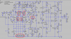
I managed to combine the JFET version and the two AllBJT versions
from post #503 on the main board.
For the JFETs an additional pad for the gate connection was added.
(the gate pin of the JFET must be bended a little).
To replace JFET 2N5462 a footprint for the SMD version MMBF5462 (SOT23) was added.
The two AllBJT versions can be selected by solder bridges. For version 1 two or four transistors can be used.
To realize the simpler AllBJT version suggested by Hans
two current sources to the neg. supply were added using SMD components.
Nevertheless some pads for connection of a daughter board have been added.
For the VAS section BC5xx / 2N2222 / MPSA18 and BD139 can be used (footprint for BD139 added).
Remarks:
Acc. to the latest simulation schematics (post #503)
C10 ( || to the 15V zener diode) was reduced from 1000uF to 100uF.
This helped me to put all input versions to the main board.
Is C30=100n || the diodes D11/D12 still required?
Hans suggested
to connect C19=1000uF to R33-2 insteadt of R33-1
to change R52 from 2k2 to 10k
Please review the attached schematic. The layout proposal will follow soon.
Cheers
Attachments
Hi Indra1,
Interesting to know that Hugh reports good results audio from adding this resistor.
Although it wasn't clear from the description that the considered the fact it increases
VCE of the driver to be greater than with just a simple cascode.
Although unless the current varies a lot it's difficult to believe that the VCE variation
is very much (47mV for 1mA change) so difficult to believe this causes instabliliy which was Max's concern.
Overall we are correcting small errors, which without correction hide detail in the sound. Or so we believe
- Symon
DearMax,
Hoping to understand you correctly, the base of the VAS Cascode sees Hfe[Q17]*(26)/Ic(ma)+R50+Ro[Q15] or approx 1.3+47+7k5.
As you can see, R50 will hardly play any role for the cascode transistor.
But for Q15 it will make a difference, because with R50 its collector will see a much larger voltage swing, combined with the effect that Vce will drop almost 1 volt (20mA*47ohm), both affecting the BW of the transistor and thus potentially stability.
As you have done all the time so far, listen to the beast and if no acoustical benefit is perceived from R50, leave it out.
Hans
Dear Hans, Symon and Indra,
Thank you for clarifying this interesting aspect of the so important VAS.
We are learning a lot.
Perhaps dear Hugh won't protest if we take the liberty of quoting him, for completeness' sake:
If VAS and its cascode run at 6.5mA, then Zin of the cascode emitter is 4R (26/Ie). This corresponds to re, of course. If we interpose a resistor and drop 200mV across it, then the value becomes 200/Ie, or 7.7 times the value of Zin of the EF. This is 31R, npv of 33R. 7.7 is suspiciously close to the accepted engineering bridging ratio of 10.
It helps both with impedance transfer from collector to emitter and linearises the input impedance of the EF, drowning it in a constant value. There appears to be no penalty for this, since voltage drop is trivial and hardly affects rail efficiency.
Quote:
When the output (output impedance) Zout of a device (the source, ZS in illustration) is connected to the input (input impedance) Zin of another device (the load, ZL in the illustration), it is a bridging connection if the second device does not appreciably load the previous device.
Essentially no power is transferred. The second device is sensitive to the output voltage of the first device, and this is maximized when loading is minimized. All good line level audio connections are bridging, to ensure the high fidelity transfer of a voltage signal from one device in the chain to the next. If the bridging criterion is not satisfied, there may be distortion, altered frequency response or both.
A connection is commonly said to be bridged if the load impedance is at least ten times the source impedance.
Though this was not my fear, this aspect is now understood. I will try to find the reference, which I seem to remember comes from Bonsai...
http://hifisonix.com/wordpress/wp-c.../Cascode-Oscillation-in-Audio-Amplifiers1.pdf
More Notes On Cascode Amplifier Oscillation
Dear JOSI1, brilliant work, as always...who would have thought at the beggining that the input section would end being so loaded with stuff!
Is C30=100n || the diodes D11/D12 still required?
I believe it is. Why?
Dear Gaetan, with that one you probably need more jumpers than parts, hehe.
Best wishes to all,
M.
Last edited:
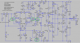
Guys, today I had some time to re-evaluate the ALLBJT versions.
The only one that works and is stable is my recommended "version 1", which has only 2 extra BJTs, each to feed a pair of equally bootstrapped BJTs, with its bases connected to the common node, previous to emitter degeneration resistors (100R; and 20R on Hans oprional version) with all other versions failing badly on the square wave test for reasons unknown to me at this time. Even the recommended "version 1" fails when one adds a couple of extra BJTs to make subcircuits completelly independent from each other...
So, for the time being, I only recommend "version 1" as working both in simulation and in real life.
While further testing, I discovered that the internal traces had "glitches" when challenged with square tests: capacitors and capacitor-resistor were tried to reduce those glitches. After doing my best, I discovered that the glitches were feed through feedback circuit and that 5p//FB resistor, already recommended by JOSI1 and Symon if I remember correctly, completelly eliminated those glitches, with square wave tests that cannot be critizised.
I hope the 4//50K big metal film resistors give some extra picoF...
Pease see attached schematic. Resistors previously 200K were increased to 400K. Please neglect the cascode on top of the added bootstrap BJT.
Other concerns: clipping behavior was not commented on the boostrap VAS, or at least I do not remember. For CCS-VAS, diodes D21 and D22 are recommended, as per others advice.
Dear JOSI1, I imagine Hans' bootstrap option will be possible on your version...
I now realize I never tried LEDs instead of Zeners for the Vref/bootstrap of the output...I simulated them both in drivers stage and in output and I think I may try them in the driver stage...no difference in THD but it may be better sounding and perhaps more stable, given what was written on Hifisonix' site about HF noise from Zeners...
Cheers,
M.
Attachments
Last edited:
Sorry to be such a PIA:
Of course those glitches and sparks also appear on the JFET input amp when challenged with the torturing square wave test. They all dissappear when using the 5pF//FBResistor plus a small 300R resistor prior to both gates of the JFETs J2-J4 (and also J1-J3 for the sake of symmetry) which can be a small SMD on the real PCB. Thus loaded, the FB loop produces fewer current spikes so when the signal arrives to J2 everything is perfect. This way I strongly believe that the amp will be unobjectionable.
Edit: I forgot to add that on this .asc file I chose the electrolytic caps most similar to my Rubycons I could find...I hope polarities are correct.
I hope you like it.
M.
I discovered that the internal traces had "glitches" when challenged with square tests: capacitors and capacitor-resistor were tried to reduce those glitches. After doing my best, I discovered that the glitches were feed through feedback circuit and that 5p//FB resistor, already recommended by JOSI1 and Symon if I remember correctly, completelly eliminated those glitches, with square wave tests that cannot be critizised.
Of course those glitches and sparks also appear on the JFET input amp when challenged with the torturing square wave test. They all dissappear when using the 5pF//FBResistor plus a small 300R resistor prior to both gates of the JFETs J2-J4 (and also J1-J3 for the sake of symmetry) which can be a small SMD on the real PCB. Thus loaded, the FB loop produces fewer current spikes so when the signal arrives to J2 everything is perfect. This way I strongly believe that the amp will be unobjectionable.
Edit: I forgot to add that on this .asc file I chose the electrolytic caps most similar to my Rubycons I could find...I hope polarities are correct.
I hope you like it.
M.
Attachments
Last edited:
- Home
- Amplifiers
- Solid State
- The AMNESIS amp: a good amplifier, like a gentleman, has no memory.