Max,
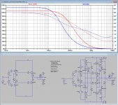
I had a closer look at the cascoded OPS.
I compared with a non cascoded version, using for as far as possible the same components, still using the 50Watt@20Khz test as before.
First of all I tried to find the optimal Quiescent current. For both versions this was at 125mA, giving resp 0.017%/Cascode and 0.022%/Straight.
When going to 75mA Quiescent current, THD20K became resp 0,047% and 0,037% or +8dB and +4.5db. The cascoded version proves to be a bit more sensitive for the right adjustment.
Next I measured the input impedance of both versions.
The straight version has a slightly higher LF impedance at 115KOhm versus 105KOhm for the cascoded version.
However as can be seen in the image below in red, the cascoded version has a significantly higher BW, which is to be preferred.
I could not find any effect caused by C36 and R39, which can be both omitted to my opinion.
As a conclusion: Cascoding the driver of the OPS, results in a better HF load for the VAS, which in turn leads to less distortion helping the Amnesis to become a top performer.
Hans
Attachments
Max,
I had a closer look at the cascoded OPS.
I compared with a non cascoded version, using for as far as possible the same components, still using the 50Watt@20Khz test as before.
First of all I tried to find the optimal Quiescent current. For both versions this was at 125mA, giving resp 0.017%/Cascode and 0.022%/Straight.
Luckily, I have bigger heatsinks!
When going to 75mA Quiescent current, THD20K became resp 0,047% and 0,037% or +8dB and +4.5db. The cascoded version proves to be a bit more sensitive for the right adjustment.
Next I measured the input impedance of both versions.
The straight version has a slightly higher LF impedance at 115KOhm versus 105KOhm for the cascoded version.
However as can be seen in the image below in red, the cascoded version has a significantly higher BW, which is to be preferred.
I could not find any effect caused by C36 and R39, which can be both omitted to my opinion.
Those proved to be useful to tame oscillation at one stage. Can be viewed as optional, probably...
As a conclusion: Cascoding the driver of the OPS, results in a better HF load for the VAS, which in turn leads to less distortion helping the Amnesis to become a top performer.
Hans
Dear Hans,
I don't know how to thank you for all your interest and energy invested in our little project. You find me in a personal low, though, with much real life interference, exhausted and with only one week ahead to summer vacation...it is hard for me to envisage complex re-organization of the circuit. For that, I simulated a quick and dirty version, with errors as you pointed out, and, as now I realize, with a fishy behavior on square wave test...trying to debug it proved hard.
I fully understand all your advices and the rationale behind them but I find it hard at the moment to grab the energy and time required to proceed to the orderly modification and testing of the circuit, especially when I consider the present state of both versions to be fully satisfactory in musical terms (I may be positively inclined to a certain amount of distortion and "dirt"
 ) and that my primordial concern was not THD in the first place...
I was hopping that the "first edition" of the amp gained enough acceptance to motivate enough people to investigate further and develop a more refined version, which I confess, may be beyond my limited capacity...I feel already payed by having a working amp, which sounds nice in addition.
In the following days I plan to do easy tries:
1) Look for my "improved current sources" article and try to find the best CCS I can for the input section.
2) Try the EF VAS again...
3) Cascode the bootstrap for the bootstrapped input section
I am glad that you analyzed the output section also. The present configuration of the "QUAD" was selected only in sonic terms as it seems not to limit the benefits of the putative LTMD organization of the previous sections, in the aspects of transparency and dynamics, which are my main goals, as I always repeat...
If you have time, can you analyze the Darlington output on post #468, which seems dearest to JOSI1?
Gratefully yours,
M.
Attachments
Last edited:
Hi Max,
As in your previous version, Q11 and Q12 have a Vce of 0Volt and cannot function as transistors.
The biggest advantage of your two stage OPS is the cascoding of the Drivers.
The Darlingtons in #476 do not have this cascoding, resulting in a higher Vas loading which is an absolute disadvantage.
From a THD point of view, cascoding the drivers seem to be much more important as cascoding the output transistors , but I have no idea what is does to the sound reproduction, a thing that cannot be measured with LTSpice.
Hans
Last edited:
Hi Max,
As in your previous version, Q11 and Q12 have a Vce of 0Volt and cannot function as transistors.
Oops! I must stop working on a hurry...
The biggest advantage of your two stage OPS is the cascoding of the Drivers.
The Darlingtons in #476 do not have this cascoding, resulting in a higher Vas loading which is an absolute disadvantage.
From a THD point of view, cascoding the drivers seem to be much more important as cascoding the output transistors , but I have no idea what is does to the sound reproduction, a thing that cannot be measured with LTSpice.
In my only experiment, which lacked inter-emitter resistor, there was some wanting of easiness to the sound, by comparison to the QUAD. I wish I could find a medium power MOSFET to make a cascode arrangement for the drivers similar to the output...
Hans
Visitors arrived. My little brother and family. Little hope for experimenting.
Have a nice musical weekend.
M.
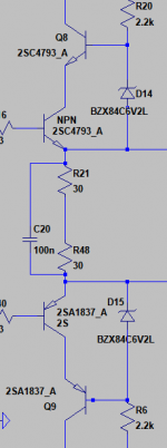
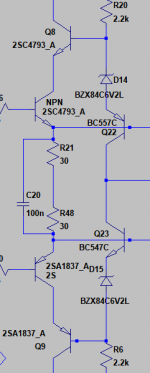
Hi Max,
as Hans says cascoding the drivers is important in terms of reducing the load on hte VAS, this was covered in Dr Arto's book, although he considered it only nessecary to cascode the driver and not the Output device as well. But as always listening testing is what counts, and I recall you reported sonic advantages to the use of mosfet cascode.
As with the input stage, driving the cascode devices Q8 & Q9 from a voltage referenced from the drivers emmitter terminal will improve things. see attached drawing, although I've not checked all the effects of this, one problem here is that the boot strape current from R6, R20, R26 & R31 directly affect the bias setting.
Or perhaps again stealing from input stage, buffer the cascode reference voltage as in my second attachment. the nice thing here is we don't need high voltage devices and they are not exposed to large voltage swings.
Anyway just thoughts at this stage.
Regaards,
Symon
Attachments
Hi Max and Hans,
allow me a short summary of the present status esp. relating to a soon layout
output / driver stage
the bootstrapped driver stage and the bootstrapped output stage (Quad) is working stable stable and provides a good sound quality.
Simpler configurations (Triple, Darlington) are possible with my latest layout by mounting options.
(R39 and C35 are kept optional)
VAS
a differential VAS is not realized yet possibly in a future step
the present state is extended by an EF option as proposed by Hans.
(With my test amp this option had no influence on stability)
JFET Input stage
the JFET bootstrapped version (post #440) is less complex and provides a good audio quality (???) if I remember correctly a statement from Max.
For J1/J2 the 2N5462 should be used. This seems to be the only JFET that provides a high value for parameter vto=-5.4.
This parameter mainly determines the negative voltage at the sources of J1/J2 and should not to be too low (J103 vto=-2.0, J74 vto=-0.54).
Fortunately the SMD version MMBF5462 is still available (e.g. at Mouser 0.30€). The optional SMD footprint is part of my layout.
(soldering the SMD device to a 3pole strip is also possible)
All BJT Input stage
is more complex and requires more components.
If I remember correctly it was a proposal from Max to increase the power supply to +-60V (JFET limit about40V).
Are there other reasons esp. sound quality to implement this more or less complex versions.
Up to now I tested successfully the less complex proposal from Hans (post #473) using BC547C/BC557C only with my test amp.
@ Hans: what was the reason to use 2N3906, 2N5550, 2N5401
(higher Uce voltage??)
For the more complex proposal of Max / Symon up to now there is no final solution in sight.
Conclusion
Diver/Output stage and VAS section are rather certain for layout.
JFET bootstrapped input section is rather certain for layout
The All BJT Input stage has to be checked and is subject to change.
For a soon layout I suggest the following procedure for the input stage:
combined layout with
- JFET bootstrapped version and
- All BJT Input stage with the less complex proposal from Hans
- provision of Solder pads / connector pins to connect a daughter board for experimenting with a more complex solutions
When I perform a quare wave test (Ua=2/3 Umax) with my test amp I still have overshots/post ringing with a tendency to heavy oscillation (some hundred KHz, no HF oscillation).
With an input filter of at least R=1K C=470p to increase output rise time >2us the amp is very stable and shows a perfect slightly rounded 20KHz quare wave.
This behaviour is present with simplest output configuration (no cascoding, no boostraping) and is indepandant from VAS / EF-VAS,
CCS-VAS / Bootstrapped VAS
@Max: did you watch this behavior at your test amp
@ Hans: I never saw an overshot in all the simulations with the pulse signal. This pulse signal generates a positive quare pulse at the amp input that then can be watched at the amp out.
My Square wave generator generates a square wave signal symmetrical to GND (pos and neg. half wave) like in case of a sine wave signal and no over shots were measured at the input of my test amp
Could this explain the difference between simulation and a real measurement.
Cheers
Several reasons, the most important one stability.Hi Max and Hans,
@ Hans: what was the reason to use 2N3906, 2N5550, 2N5401
(higher Uce voltage??)
I always test without input filter cap with 0.4Vin and 0.2usec rise and fall time. Especially the CFP transistor has to be very fast to prevent oscillations, there I used the 5550 or even better the 5551 with a higher Hfe.
I used the 2N3904 for the input, because there is a cheap dual in SOT package giving large benefits in temp distortion.
And I used the 5401 because of the much higher voltage margin. Don't use transistors at their edge. especially when switching on or off they may die.
Because Fets are usually so much faster, you wont have as much sttability problems, but matching will be another problem and of course the restricted voltage reach.
What are those differences ? symmetrical or non symmetrical should not make a big difference, but be careful in real life to keep the amplitude low, not to blow your zobel network and preferably loaded with an 8 Ohm resistor.@ Hans: I never saw an overshot in all the simulations with the pulse signal. This pulse signal generates a positive quare pulse at the amp input that then can be watched at the amp out.
My Square wave generator generates a square wave signal symmetrical to GND (pos and neg. half wave) like in case of a sine wave signal and no over shots were measured at the input of my test amp
Could this explain the difference between simulation and a real measurement.
Cheers
Hans
Thank you guys, wholeheartedly, to come to my rescue.
Dear Symon,
The first arrangement was tested at some point but it did not go well...
The second one is very interesting but first simulation showed poorer results...
Dear JOSI1,
Excellent summary of the "State Of The Project" (SOTP; sorry... I must stop watching political videos )
I concur with your views.
Output section: is a good starting (or end) point, and could be built progressively from simpler to more complex, if you wish so.
VAS: today I plan to re-assault the EF VAS with BC546-->N222X cascoded with "SC4793, which gave good performance in the attached simulation.
Since the original LTMD schematic from Peufeu was simple cascoded common emitter, I wonder if the putative LMTD is jeopardized...we'll see...or hear better.
Input section: my JFET version is sounding good an is stable with J74 and J103 with 32V supplies. I am inclined to think that, when buying a good amount of J103 one will find several units whose gain is more near 4mS...I have somewhere a practical test circuit.
My ALLBJT version with activelly bootstraped CFP is sounding good. This version, which is a modification from Symon's clever idea, is very dynamic. At least we should have connecting points for daughter-boards at the critical points, those being the emitters and the common node before the degeneration resistor, which is my present option.
Dear Hans,
Regarding Q11-Q12, my previous simulation showed 100mV of Vce and the present one increased to 200mV with different LEDs, which seems enough for LTspice: that reinforces the notion that searching for the optimal (THD; stability and soundwise) operating points is crucial, hence the recommendation of using variable resistors at first to set those points, in case one want to use ALLBJT, letting for a second time fitting LED alone or in combination or whatever units you prefer.
Regarding the optional transistor types, I let you inform us the better ones and it is up to JOSI1 to provide for the most versatile PCB possible to accomodate those.
Regarding tests: I am usually too excited with a good sounding mode to test the square wave in real life I may remember today.
Soooo, I am ready if you are.
Be prepared to face the unknown, though; be brave and do not despair!
(don't Panic!)
Best wishes,
M.
Dear Symon,
The first arrangement was tested at some point but it did not go well...
The second one is very interesting but first simulation showed poorer results...
Dear JOSI1,
Excellent summary of the "State Of The Project" (SOTP; sorry... I must stop watching political videos
)I concur with your views.
Output section: is a good starting (or end) point, and could be built progressively from simpler to more complex, if you wish so.
VAS: today I plan to re-assault the EF VAS with BC546-->N222X cascoded with "SC4793, which gave good performance in the attached simulation.
Since the original LTMD schematic from Peufeu was simple cascoded common emitter, I wonder if the putative LMTD is jeopardized...we'll see...or hear better.
Input section: my JFET version is sounding good an is stable with J74 and J103 with 32V supplies. I am inclined to think that, when buying a good amount of J103 one will find several units whose gain is more near 4mS...I have somewhere a practical test circuit.
My ALLBJT version with activelly bootstraped CFP is sounding good. This version, which is a modification from Symon's clever idea, is very dynamic. At least we should have connecting points for daughter-boards at the critical points, those being the emitters and the common node before the degeneration resistor, which is my present option.
Dear Hans,
Regarding Q11-Q12, my previous simulation showed 100mV of Vce and the present one increased to 200mV with different LEDs, which seems enough for LTspice: that reinforces the notion that searching for the optimal (THD; stability and soundwise) operating points is crucial, hence the recommendation of using variable resistors at first to set those points, in case one want to use ALLBJT, letting for a second time fitting LED alone or in combination or whatever units you prefer.
Regarding the optional transistor types, I let you inform us the better ones and it is up to JOSI1 to provide for the most versatile PCB possible to accomodate those.
Regarding tests: I am usually too excited with a good sounding mode to test the square wave in real life
I may remember today.Soooo, I am ready if you are.
Be prepared to face the unknown, though; be brave and do not despair!
(don't Panic!)
Best wishes,
M.
Attachments
Last edited:
OK. Had a little time. Tried the EF VAS, with MPSA18 instead of 2N2222 which has not arrived yet...
One try: +/- 500mV oscillation high MHz.
Since I was not on the mood, I did not try to debug it. Maybe with 2N2222 and the new PCB it will be OK...
Good part is that now I have the little MPSA18 (instead of BD139) as common emitter VAS (cascoded with 2SC4793) and it is stable. Listening test ongoing.
I think I found a good .model of the said BJT...
Cheers,
M.
One try: +/- 500mV oscillation high MHz.
Since I was not on the mood, I did not try to debug it. Maybe with 2N2222 and the new PCB
it will be OK...Good part is that now I have the little MPSA18 (instead of BD139) as common emitter VAS (cascoded with 2SC4793) and it is stable. Listening test ongoing.
I think I found a good .model of the said BJT...
Cheers,
M.
Hi Max,
Just an observation, MPSA18 is a very good device, low noise and high gain at low current. It also has low Cob.
As such it is usually chosen as input device, although how well suited it is to this circuit in positions Q3 and Q5 would need to be tested, and probably feedback resistor values modified.
The high gain of this device in such a complex circuit can cause oscilation, so increasing values of feedback resistors, and adjusting bias levels may be required in any location to get hte best from it.
Regards,
Symon
Thanks, dear Symon,
Fortunately, the amp is still very stable. It is a nice transistor indeed. It can be used at input but as the NPN for the CFP. Simulations did not outperformed the previous, though. Besides, Hans and JOSI1 have given enough recommendations about different options there to be occupied for a long time...
You see, it is astonishing how the flavor of the sound can change with a tinny mod.
Burning-in is still going on for the MPSA18. I am not sold on it yet. I can advance that it sounds indeed more delicate, detailed, refined and articulated than the BD139 in that position, but I miss some of the raw power sensation and bass of the former, which sounds a bit primitive by comparison. The sound is too tight for my taste at the moment...
It only sees 22mW of dissipative stress.
BTW, I tried 2N2222 and 2N2907 on the Sziklai bootstrapped output, since the input transistors see around 10mW of stress there, thinking that they will be excellent. Well, the simulations are awful, reminding me that the Sziklai output is more a balance act than the rest of the output options...
Cheers,
M.
PS: isn't this the best hobby ever???
Hi Max,
I know what you mean about small chnages agffecting character of the sound.
I spent a lot of time modifying a CD player, and was interesting how the sound
changed with even components not obviously in signal path.
I'm not surprised MPAS18 and BD139 sound different they have very
different characteristics. I would have thought something like BC337
would be more appropreate in this position. It is more of a driver than MPSA18
but faster and more gain than BD139. But only listening will show how it sounds.
Happy listening
- Symon
Hi Max,
I know what you mean about small chnages agffecting character of the sound.
I spent a lot of time modifying a CD player, and was interesting how the sound
changed with even components not obviously in signal path.
I'm not surprised MPAS18 and BD139 sound different they have very
different characteristics. I would have thought something like BC337
would be more appropreate in this position. It is more of a driver than MPSA18
but faster and more gain than BD139. But only listening will show how it sounds.
Happy listening
- Symon
Yesterday I had another Van der Graaf Generator marathon and I am happy to say that the dynamics and bass are coming back. Understand, I am not saying that this tinny unit needs a lot of heavy action to burn-in: it is the case that when doing quick and dirty mods I sometimes overdo my soldering and heavy lumps of new metal end up on the signal track...
Interesting comment about BC337. I am sure there are lot of possibilities for this critical VAS position, so it is recommended to put there connector pins to allow easy swapping of different units to evaluate sonic presentation differences. One can find then a sound balance that better match one's taste.
MPSA18 has Cbc of 1,5pF and Ceb of 5,6pF, typical, as per datasheet.
Another aspect to evaluate is average working temp (not instant T° change of the junctions) as, per convenience, I had the BD139 attached to the heatsink from the 2SC4793 cascode which does all the heavy work, sharing its T° behavior. So the BD139 was warmer than needed...could this influence sound balance? I guess the answer could be positive. It should be easy to perform an ear test...
Cheers,
M.
Filter IT. I hate Solid State...Low voltage has hardly no Power or Energy....They Require LOTS of Capacitance and for Smoothing/Ripple Rejection.
A couple 6800uf's do not Sound good at all lol. I will Replace with Audio Grade 10,000uf.
Thanks for the post JRZoid, but I do not know why you are here if you hate SS, with all due respect...
For the record, we are exploring strategies to avoid or reduce LTMD, and hope this will aproach SS to Tubes, while keeping the advantages of SS over Tubes.
Cheers,
M.
Dear Max,
I don’t doubt for even a second your impression that changing the VAS transistor changed the sound perception.
However I find it hard to understand how one single transistor could have this noticeable effect.
Therefore my question: do you still have an old transistor radio.
This is a perfect tool to detect HF oscillations in the Mhz region without invading or loading the amp and if not excludes that HF is changing the perceived sound.
Hans
Last edited:
Dear Max,
I don’t doubt for even a second your impression that changing the VAS transistor changed the sound perception.
However I find it hard to understand how one single transistor could have this noticeable effect.
Therefore my question: do you still have an old transistor radio.
This is a perfect tool to detect HF oscillations in the Mhz region without invading or loading the amp and if not excludes that HF is changing the perceived sound.
Hans
Yes. You are most probably rigth. I already thought about this possibility and dear Symon commented about it also. This amp has still the SMPS supply which has those bursts of oscillation that surelly are a too big test for any amp, and probably I have bursts of oscillation that I am not catching on the scope and that is the reason why there is perception of unbalanced sound to the mid-highs. I did not had the time to transplant the linear PS that I have spare.
But I am officially on vacation for two hours now
so I will revert to the last version for now and then when the linear supply is installed I will try again.The other amp, the red PCB, has a linear supply ("charge-transfer supply"), without noises and I will try the mod there, which shall be faster to do.
Ostripper wrote:
Even 4700uf is good( sounds good ? subjective) if it is bypassing 70KHZ rectification.
That would be SMPS. I'm permanently out of the big trafo 100,000uf
"fetish". No more " boat anchor" SS power amps.
OS
My good SMPS (not the present one) sounds nice with added capacitance.
Usually 10.000uF per side. On this one I used 20.000. Perhaps that caused the malfunction...
Anyway for 35W you don't need more...
Cheers,
M.
Input stage
I'm working on a combined layout for the JFET and AllBJT input stage.
There exist several versions for the AllBJT input which are more or less complex. It's not possible to cover all the versions on the main board. The complex versions which are not perfect yet and subject to change must be shifted to a daughter board.
I tested successfully the proposal from Hans (post #475 using only BC5xx transistors) with my test amp.
@ Hans: Why do use 3 LEDs for D1/D2. Simulation shows the same result for THD when using only one LED.
The latest proposal from Max/Symon (post #488) differs completely from proposal (post #476).
@Max: Is proposal (post #488) your favorite now.
Simulations show that the voltage drop across the LED/Diodes is
very critical for the functionality.
When increasing the voltage drop D16/D11/D13 to increase Uce for Q11/Q12 the simulation does not work.
Is it advising to use LED LXK2-PW14 which is a power LED (Vf=3.6V @350mA) for simulation.
Which components did you use for D9 and D16/D11/D13 in your test amp for listening tests (the LEDs used for simulation are not suited for a real amp or hard to order).
Beneath providing solder pads for connecting a daughter board I'm looking to find AllBJT versions that can be placed on the main board.
One candidate is the proposal from Hans. Max do you have another proposal which is not too complex.
Output stage
Emitter resistors R9/R12 are 0.3 Ohm for simulation.
Can I use 0.22 Ohm or better 0.33 Ohm for real amp?
The optimal quiescent current (125mA) will be measured as voltage drop across R9 or R11??
Depends the optimal quiescent current from the used resistor value
(0.3/0.22/0.33 Ohm)??
Cheers
- Home
- Amplifiers
- Solid State
- The AMNESIS amp: a good amplifier, like a gentleman, has no memory.