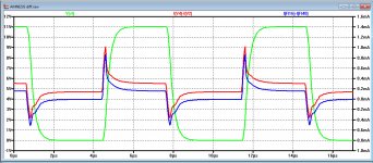
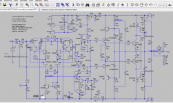
And as a final confirmation that everything is o.k., in the image below one can see the difference in the two driving line currents I(V2) and I(V4) versus the difference in the driver base currents through R16 and R40.
They are equal, just as expected.
Hans
They are equal, just as expected.
Hans
Attachments
Oh! I see there has been some action here. ")
At this stage and given the previous argumentation in favor of a differential VAS maybe it would be wise and take a step back.
1) It would potentially be the better technical answer (especially if we can add those SMD drivers; see attached) though we have not an idea about how it will sound.
2) I do not have experience with this, safe what I can learn from literature, so you guys will have to design this part, if the interest climbs...
3) This will make for a completelly changed PCB.
So, maybe it is time to think about the initial project as it is with through hole units, like a stage 1, or proof of concept project, and then, if the amp is declared worthy of further development, proceed to a stage 2, with more complex circuitry and possibly SMD solutions.
I see that those two projects might appeal to different DIYers.
What do you think?
Cheers,
M.
PS: I forgot to thank you for your kind explanation.
The only purpose of R1 is to keep the amps output offset under control when no source is connected.
The output impedance of the voltage source V3 in parallel to R1 is 0 Ohm, that's why you see no difference.
With Fets you could even go higher, but 100K seems a practical value.
Attachments
Last edited:
Hi Max,
I agree with you to go this way.
For the moment I would prefer a variant with single JFETs with a JFET input to use R1=100k.
In addition it should be possible to add a future SMD variant now. This however requires that the previous solution with transistor + 4 diodes is obsolet now.
(Btw JFET 2N5462 is discontinued and hard to get).
But a differential VAS would need a completely new layout with with more board space.
For the driver stage a can try to add 2SCR514P/2SAR514P in parallel to
BD139/BD140.
What about the driver cascodes. Is the use of BD139/BD140 fixed now or
is the use of 2SC4793/2SA1837 still an option. Due to the reversed pinout
and mounting to a heatsink it is not possible to provide a layout for both.
Lately a 50 Ohm resistor was added again between driver and cascode.
Cheers
So, maybe it is time to think about the initial project as it is with through hole units, like a stage 1, or proof of concept project, and then, if the amp is declared worthy of further development, proceed to a stage 2, with more complex circuitry and possibly SMD solutions.
I agree with you to go this way.
For the moment I would prefer a variant with single JFETs with a JFET input to use R1=100k.
In addition it should be possible to add a future SMD variant now. This however requires that the previous solution with transistor + 4 diodes is obsolet now.
(Btw JFET 2N5462 is discontinued and hard to get).
But a differential VAS would need a completely new layout with with more board space.
For the driver stage a can try to add 2SCR514P/2SAR514P in parallel to
BD139/BD140.
What about the driver cascodes. Is the use of BD139/BD140 fixed now or
is the use of 2SC4793/2SA1837 still an option. Due to the reversed pinout
and mounting to a heatsink it is not possible to provide a layout for both.
Lately a 50 Ohm resistor was added again between driver and cascode.
Cheers
I JOSI1,
Look inside.
Have you experienced problems with the N2222 VAS transistor?
Thanks so much,
M.
Look inside.
Hi Max,
I agree with you to go this way.
OK.
For the moment I would prefer a variant with single JFETs with a JFET input to use R1=100k.
Any JFET with gate center pin should be inter-changeable with BD550 and family. This project in principle is an all-BJT amp which should be inexpensive and affordable to attract a potentially higher number of enthusiasts. All our last exercises are higher priced refinements, technically probably better but whose sound cannot be predicted. The aims for the amp were (are) transparency and dynamics. The more complex solutions probably will be more transparent but I suspect dynamics will suffer...so it's risky.
In addition it should be possible to add a future SMD variant now. This however requires that the previous solution with transistor + 4 diodes is obsolet now.
(Btw JFET 2N5462 is discontinued and hard to get).
No, the 4 diode (may be 3) version is not obsolete. Due to real life obligations, I've not had the time to compare side by side both amps (cascoded-CFP with "BJT and 4 diodes" v/s bootstrapped-CFP with JFET (BTW I wonder if my diodes are faulty. They measure well but fail to keep the expected potential difference...) but I might do it this weekend.
But a differential VAS would need a completely new layout with with more board space.
That is what I feared. A modular approach would be also tooo complex...
For the driver stage a can try to add 2SCR514P/2SAR514P in parallel to
BD139/BD140.
That would be nice, but has anybody used those before? I bet they can stand the power dissipation on driver duty.
What about the driver cascodes. Is the use of BD139/BD140 fixed now or
is the use of 2SC4793/2SA1837 still an option. Due to the reversed pinout
and mounting to a heatsink it is not possible to provide a layout for both.
Yes, pinout poses a problem. I confess I mount them from the belly when Vce is low
I need advice here: BD139/140 are good as cascodes as long as the amp does not oscillate heavily. If it does, probably they will blow and it is not funny to desolder and dismantle again and again. Minor amplitude oscillation is OK. That is why I tend to prefer bigger BJTs that could withstand more heat for short lapses, at the risk of increased THD.
Lately a 50 Ohm resistor was added again between driver and cascode.
Those were added as the .models were behaving not as expected for the 4793/1837 units. Forget them please.
Cheers
Have you experienced problems with the N2222 VAS transistor?
Thanks so much,
M.
At this stage and given the previous argumentation in favor of a differential VAS maybe it would be wise and take a step back.
Hi Max,
I just wanted to plant a seed in your mind because you have invested so much time in Stage 1 and 3 and relatively less in Stage 2, the VAS.
But knowing all the options it is easier to take the decision you prefer.
Maybe its nice to know that at least Mark Levinson uses differential VAS amps since their beginning.
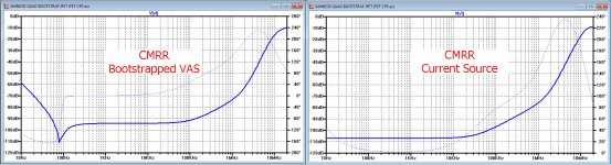
One last thing concerning the VAS.
In the current version, you have applied a bootstrap.
When changing R3 into a current source, PSRR from the positive supply line will increase significantly, especially at the low end of the FR.
Look at the image below.
I hope you don't get annoyed being fed with ideas ?
Hans
Attachments
Last edited:
Dear Hans,
"Look inside".
Thanks a lot,
M.
"Look inside".
Hi Max,
I just wanted to plant a seed in your mind
I know and I thank you.
because you have invested so much time in Stage 1 and 3 and relatively less in Stage 2, the VAS.
My hope was that you guys helped me to optimize the bootstrapped VAS
But knowing all the options it is easier to take the decision you prefer.
Maybe its nice to know that at least Mark Levinson uses differential VAS amps since their beginning.
Nice. But logistically speaking it is preferably to go from "simpler" to more complex solutions. Remember that I am the only human being that has listened to the monster and I could be totally wrong in my sensing or our tastes could be totally opposite. That being said, It would be nice if stage 2 Amnesis have not only diffrential VAS but also parallel power units to go higher in machoness, not that I feel it is needed...
One last thing concerning the VAS.
In the current version, you have applied a bootstrap.
When changing R3 into a current source, PSRR from the positive supply line will increase significantly, especially at the low end of the FR.
Look at the image below.
Yes, we have the CCS with Hawkford's option still in place, don't we JOSI1?
I hope you don't get annoyed being fed with ideas ?
Not in the least. "I live to Learn"
I am an addict and learning is my droug...
Hans

Thanks a lot,
M.
Last edited:
Hi Max,
Here is a third alternative, with the upper two fets replaced by bipolars.
I have tested IMD 19Khz+20Khz for both versions in open loop while in that mode it it easier to find the differences.
Output voltage ca +/-21Volt max.
The distortion figures are in favour for the Bipolar version, especially the not so nice IMD product at 1Khz.
Question: You have used 4 * 50K in the feedback loop. Are you really using 4 resistors at this spot ?
Hans
Attachments
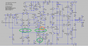
The current source for the input pair has a 83 Ohm resistor in the left image instead of the 100 Ohm in the right circuit.
This has only to do with the fact that I used 2*1N4148 versus 2 generic diodes.
Since they differ in voltage, I had to adjust the 100 Ohm to 83 Ohm to get exactly the same 6.66mA tail current for both versions.
Hans
This has only to do with the fact that I used 2*1N4148 versus 2 generic diodes.
Since they differ in voltage, I had to adjust the 100 Ohm to 83 Ohm to get exactly the same 6.66mA tail current for both versions.
Hans
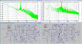
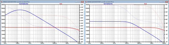
Dear Max,
There are schools that propagate that the loop gain should be flat from 20Hz to 20Khz.
This is easy to achieve with the latest Bipolar/Fet version, because open loop gain is high enough.
When placing 500K in series with 100nF parallel to the Miller cap, the gain of the VAS will be linearized and reduced, but because of the feedback through this 500K, distortion will even drop.
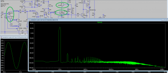
In the images below you see the Loop gain in blue and overall gain in red.
Left image is as-is. The low frequency drop in loop gain is because of the used Bootstrap.
The image at the right is with the linearized VAS with 500K + 100nF parallel to C10 being 20pF in this case.
Loopgain has its -3dB point now at 20Khz.
A very simple trick to use, with sometimes surprising effect on sound reproduction.
N.B. Open loop gain = Closed loop gain + Loop gain.
Hans
There are schools that propagate that the loop gain should be flat from 20Hz to 20Khz.
This is easy to achieve with the latest Bipolar/Fet version, because open loop gain is high enough.
When placing 500K in series with 100nF parallel to the Miller cap, the gain of the VAS will be linearized and reduced, but because of the feedback through this 500K, distortion will even drop.
In the images below you see the Loop gain in blue and overall gain in red.
Left image is as-is. The low frequency drop in loop gain is because of the used Bootstrap.
The image at the right is with the linearized VAS with 500K + 100nF parallel to C10 being 20pF in this case.
Loopgain has its -3dB point now at 20Khz.
A very simple trick to use, with sometimes surprising effect on sound reproduction.
N.B. Open loop gain = Closed loop gain + Loop gain.
Hans
Attachments
Hi Max,
Here is a third alternative, with the upper two fets replaced by bipolars.
I have tested IMD 19Khz+20Khz for both versions in open loop while in that mode it it easier to find the differences.
Output voltage ca +/-21Volt max.
The distortion figures are in favour for the Bipolar version, especially the not so nice IMD product at 1Khz.
OK. Great. That will safe us some money. Can you by chance simulate the "cascoded-with-4diode CFP input"?
Question: You have used 4 * 50K in the feedback loop. Are you really using 4 resistors at this spot ?
Yes. I have the other amp with a lonely 12K resistor
Hans
The current source for the input pair has a 83 Ohm resistor in the left image instead of the 100 Ohm in the right circuit.
This has only to do with the fact that I used 2*1N4148 versus 2 generic diodes.
Since they differ in voltage, I had to adjust the 100 Ohm to 83 Ohm to get exactly the same 6.66mA tail current for both versions.
OK. I got it.
There are schools that propagate that the loop gain should be flat from 20Hz to 20Khz.
This is easy to achieve with the latest Bipolar/Fet version, because open loop gain is high enough.
When placing 500K in series with 100nF parallel to the Miller cap, the gain of the VAS will be linearized and reduced, but because of the feedback through this 500K, distortion will even drop.
In the images below you see the Loop gain in blue and overall gain in red.
Left image is as-is. The low frequency drop in loop gain is because of the used Bootstrap.
Great trick!
Like what I post?
I tried to update to what I am using in the "red PCB" amp. That one is using now the fat 4793/1837 driver and cascodes. The amp is stable so far (one week) and it sounds warmer than with BD139/140, maybe due to increased 2nd harmonic (?)...besides, I forgot that I had bought a couple of bags of those fat drivers
The image at the right is with the linearized VAS with 500K + 100nF parallel to C10 being 20pF in this case.
Loopgain has its -3dB point now at 20Khz.
A very simple trick to use, with sometimes surprising effect on sound reproduction.
N.B. Open loop gain = Closed loop gain + Loop gain.
Hans
Thanks so much.
M.
Attachments
I have inserted the 2SJ74, which performs quite well.
Also the 2SC4793 and the 2SA1837 in the drivers perform much better as the BD139C/BD140C.
The input filter that I used is less rigorous as what you advised, but yours can also be used.
But the 100pF Miller cap reduces the loop gain to be flat to 4Khz instead of to 20Khz, so try to use the 20pF cap.
Hans
Attachments
I have inserted the 2SJ74, which performs quite well.
My .models might be wrong, then...can you upload the .lib file please?
Also the 2SC4793 and the 2SA1837 in the drivers perform much better as the BD139C/BD140C.
Great to know. Again, my .models do not behave properly...there is a case to prefer BCE pinout transistors then
The input filter that I used is less rigorous as what you advised, but yours can also be used.
But the 100pF Miller cap reduces the loop gain to be flat to 4Khz instead of to 20Khz, so try to use the 20pF cap.
Yeah. I forgot to comment that that linearization of the VAS trick may allow us to soften the other "stabilization" methods, like lower Miller, lower gate stopper resistors, higher corner input filter, maybe get rid of the RC filter for the driver's cascode...
Hans
Edit: Hey! I don't see the RC // to Miller...did I get it right???
Many thanks. I will see if I can play a little tomorrow...
M.
Last edited:
Hi Max,
Edit: Hey! I don't see the RC // to Miller...did I get it right???
Many thanks. I will see if I can play a little tomorrow...
M.
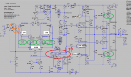
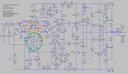
RC // Miller was included indeed, see red circles.
I have included a zip file with the .asc and the .lib file, keep them together in the same folder.
There was a reason why I asked for the 4*50K feedback resistor.
This resistor position is the most sensitive in the whole amp and should at least be a 0.5W metal film resistor.
If not you will have a lot of added distortion because even a resistor is not the ideal linear component you would expect it to be.
Hans
Attachments
For added stability you could, only if you need, add a 47pF cap with 100 Ohm in series between the drains of J1 and J2.
This has no effect on the loop gain up to 20Khz.
The other thing I forgot to mention is that in the simulation R43/R44 in the mosfet gates, 10 Ohm gives a (slightly) better step response as the 130 Ohm you are using currently.
Hans
This has no effect on the loop gain up to 20Khz.
The other thing I forgot to mention is that in the simulation R43/R44 in the mosfet gates, 10 Ohm gives a (slightly) better step response as the 130 Ohm you are using currently.
Hans
Hi Max,
RC // Miller was included indeed, see red circles.
I have included a zip file with the .asc and the .lib file, keep them together in the same folder.
Thanks!
I am not used to your shortcuts...
There was a reason why I asked for the 4*50K feedback resistor.
This resistor position is the most sensitive in the whole amp and should at least be a 0.5W metal film resistor.
If not you will have a lot of added distortion because even a resistor is not the ideal linear component you would expect it to be.
My 4 // resistors, each high quality, are equivalent to 2,4W but at shorter length.
I know the limits, that's why I wound my own DIY honeycomb resistors for I/V conversion
Hans
Thanks very much. Another post to follow...
M.
For added stability you could, only if you need, add a 47pF cap with 100 Ohm in series between the drains of J1 and J2.
This has no effect on the loop gain up to 20Khz.
Thanks.I attached new schematics: for your last version I named it "JFET BOOTSTRAPPED INPUT"; the other one is the previous "BJT CASCODED INPUT".
Due to logistics I preferred to mod the BJT cascoded input amp with the new VAS compensation. I realized that I don't have 20pF caps plus this one shows peaking at 10MHz so I chose 39pF to start.
Edit: with reduced Mosfet's gate stopper resistors to 10R the peaking is reduced!
The JFET bootstrapped input shows impressive simulations. Fortunatelly, both versions can be built on the same JOSI1-PCB
The other thing I forgot to mention is that in the simulation R43/R44 in the mosfet gates, 10 Ohm gives a (slightly) better step response as the 130 Ohm you are using currently.
Yes. That I was saying by re-studying the optimal values now that the .models seem to work.
Hans
A thousand thanks.
M
Attachments
Last edited:
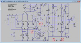
Max,
The resistor you have encircled in orange, is use by me to change from 1e9 into 1e-9, in that case showing the open loop gain of the amp.
The Voltage source V2, is to measure the loop gain in a closed loop situation.
Put 1 Volt on it, and divide the voltage on one side by the other side and you get this loop gain.
Hans
Max,
The resistor you have encircled in orange, is use by me to change from 1e9 into 1e-9, in that case showing the open loop gain of the amp.
The Voltage source V2, is to measure the loop gain in a closed loop situation.
Put 1 Volt on it, and divide the voltage on one side by the other side and you get this loop gain.
Hans
Dear Hans,
Thanks very much for answering my unspoken question...
I'll let those considerations to your expert evaluation, better...
I think that, with the behavior below shown, the JFET bootstrapped input with the big 4793/1837 drivers and cascodes should be a good bet to go into "production".
For those who do not want to invest in JFETs at all, there is also the possibility of an "all-BJT input section", shown in attachment, inspired by the re-reading of Hephaïstos' patent, which includes much more complex organizations...the V1 voltage source can be set with different voltages to test the overall behavior and can be configured with different sub-circuits, including deriving it from the same (even a single) sub-circuit of the internal CFP cascode to save on parts.
What do you guys think?
Cheers
M.
Attachments
Last edited:
- Home
- Amplifiers
- Solid State
- The AMNESIS amp: a good amplifier, like a gentleman, has no memory.