
You can make a VFA with gain-bandwidth independence by returning the Miller compensation capacitor from the VAS collector to the inverting input. Now the unity loop gain frequency is a product/function of the output stage gain (typically unity), Rf and Cmiller. Change the closed loop gain by varying Rg and ensure that the inner (Miller) loop is compensated for the lowest desired gain.
A bewitchingly beautiful theory. (Beauty is the splendor of truth)
Here we go once again...
The naming originates from and exclusively refers to input terminal characteristics. The high current emitter (through the emitter-collector) serving as the input terminal for feedback designates CFA, and the low current base (through the base-emitter) serving as the input terminal for feedback designates VFA. Everything else (feedback network, energy level, CCS, buffers, whatever) being irrelevant.
However, some painful epistemological questions still remain:
In what sense is local feedback a feedback? What is fed back from what to what? How can an entity form a loop with itself? Is the notion of feedback necessary to describe the base-emitter diode?
For those who would like to use it, here my final very easy to use vehicle to determine whether a circuit(design) is a CFA or a VFA.
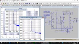
Thanks to Jan Didden for an undocumented tip, I could use two 1K feedback resistors for DC, for zeroing the output voltage.
But for AC these resistors have a value of 1Gig ! With a 1F cap in between, this set up can be regarded as open loop.
Two practical resistor values, resp. 500 Ohm and 5 K were used for Rg in a .step command.
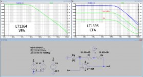
Two examples are added, one for a LT1364 VFA, being a buffered CFA and one for a LT1395 CFA,
In case of the VFA all curves are on top of the open-loop gain.
For a CFA, you can see two separate curves in Green for V(out), for resp the two mentioned values for Rg, resp. 500 Ohm and 5K.
The upper curve in blue represents the open-loop.
From the green CFA curves one can calculate Z(s).
When being uncertain whether a circuit belongs to one or the other category, you could use this tool, but you can just as well use it to simply measure OL gain and GBW.
It may also be useful for those being sceptical whether a CFA really differs from a VFA, just as you like.
Hans
Thanks to Jan Didden for an undocumented tip, I could use two 1K feedback resistors for DC, for zeroing the output voltage.
But for AC these resistors have a value of 1Gig ! With a 1F cap in between, this set up can be regarded as open loop.
Two practical resistor values, resp. 500 Ohm and 5 K were used for Rg in a .step command.
Two examples are added, one for a LT1364 VFA, being a buffered CFA and one for a LT1395 CFA,
In case of the VFA all curves are on top of the open-loop gain.
For a CFA, you can see two separate curves in Green for V(out), for resp the two mentioned values for Rg, resp. 500 Ohm and 5K.
The upper curve in blue represents the open-loop.
From the green CFA curves one can calculate Z(s).
When being uncertain whether a circuit belongs to one or the other category, you could use this tool, but you can just as well use it to simply measure OL gain and GBW.
It may also be useful for those being sceptical whether a CFA really differs from a VFA, just as you like.
Hans
Attachments
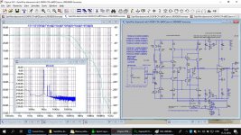
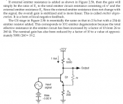
The same CFA preamp but now with 30dB of the Loop Gain instead 52dB as was in my previous post. Distortion increases and character of the harmonics changed. Now third harmonic is higher then second, but still below ppm.
The LG here can be changed by changing the R48 value(I/V converter).
I think that the way how DC servo is connected is quite novel, at least I never saw that way.
The LG here can be changed by changing the R48 value(I/V converter).
I think that the way how DC servo is connected is quite novel, at least I never saw that way.
Attachments
Hi Ian,
I waited answering you till I had finalised my version in #1465, which is a easier to use and without some difficulties the DIT might present.
Coming back to your #1432, I agree that you can go all directions with both topologies, but in defend, the circuit was meant originally by Middlebrook to be used with Rf=Rg=1k.
With that restriction it works quite well for VFA and CFA circuits.
But with low values of Rg, DIT makes a CFA look like a VFA.
The other way round whith huge values for Rf and Rg to turn a VFA into a CFA is rather far from home and will not be the preferred way of use.
My test in #1432 is much simpler in that respect, practically open-loop and with only two values for Rg, resp 500 Ohm and 5 K, that's it.
But to come back to the reason why I started this testing rig discussion, was to bring discussions to a point where one could accept that there are two different types of amplifier circuits, a CFA and a VFA.
Because after so many postings, noses are still not all in the same direction, so my proposal was to stop the discussion whether those names are semantically well chosen, bus to simply accept that one is called a CFA and the other one VFA.
And for that you need a tool to identify, voila.
Hans
Miller compensation.
You can make a VFA with gain-bandwidth independence by returning the Miller compensation capacitor from the VAS collector to the inverting input. Now the unity loop gain frequency is a product/function of the output stage gain (typically unity), Rf and Cmiller. Change the closed loop gain by varying Rg and ensure that the inner (Miller) loop is compensated for the lowest desired gain.
Yes, notice the choice of words.
") Not mine BTW, I mildly objected.
Not mine BTW, I mildly objected.Attachments
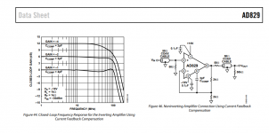
Miller compensation.
You can make a VFA with gain-bandwidth independence by returning the Miller compensation capacitor from the VAS collector to the inverting input. Now the unity loop gain frequency is a product/function of the output stage gain (typically unity), Rf and Cmiller. Change the closed loop gain by varying Rg and ensure that the inner (Miller) loop is compensated for the lowest desired gain.
Thanks for making the conditions for VFA operation clear.
Back to 101 basics
It is worthwhile going back to 101 basics as it is related to how a CFA operates.
Attached is Bob Cordell's p20 on emitter degeneration. When the emitter resistor is added the base-emitter voltage is reduced by this voltage: Vbe=Vin - Ie*Re hence negative feedback is occurring.

Since all the voltage across Re reduces Vbe it is said to be 100% voltage feedback.
Since the emitter resistor voltage is proportional to emitter current it can also be called "current feedback"
Accordingly, a degenerated common emitter stage could be called a primitive form of a current feedback amplifier or CFA (although that is not explicitly stated in textbooks or literature that I have seen).
Then, it's one step more to add a second transistor to make a CFP to arrive at the basic structure of the CFA as we know it, and the same underlying principles of degeneration feedback are still present, except a second feedback network Rf and Rg can be added to set the voltage gain.
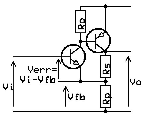
In the CFP cum CFA (courtesy of Ketje) 'Rp' is also the emitter degeneration resistor (called 'Rg' in earlier posts and articles).
An understanding of the basic common emitter stage with degeneration is needed to understand the CFP and hence the CFA as we know it.
Thanks for asking.
Sorry, I don't understand what you are asking in your last question, "Is the notion of feedback necessary to describe the base-emitter diode?
Cheers,
IH
Hi N101N,...In what sense is local feedback a feedback? What is fed back from what to what? How can an entity form a loop with itself? Is the notion of feedback necessary to describe the base-emitter diode?
It is worthwhile going back to 101 basics as it is related to how a CFA operates.
Attached is Bob Cordell's p20 on emitter degeneration. When the emitter resistor is added the base-emitter voltage is reduced by this voltage: Vbe=Vin - Ie*Re hence negative feedback is occurring.
Since all the voltage across Re reduces Vbe it is said to be 100% voltage feedback.
Since the emitter resistor voltage is proportional to emitter current it can also be called "current feedback"
Accordingly, a degenerated common emitter stage could be called a primitive form of a current feedback amplifier or CFA (although that is not explicitly stated in textbooks or literature that I have seen).
Then, it's one step more to add a second transistor to make a CFP to arrive at the basic structure of the CFA as we know it, and the same underlying principles of degeneration feedback are still present, except a second feedback network Rf and Rg can be added to set the voltage gain.
In the CFP cum CFA (courtesy of Ketje) 'Rp' is also the emitter degeneration resistor (called 'Rg' in earlier posts and articles).
An understanding of the basic common emitter stage with degeneration is needed to understand the CFP and hence the CFA as we know it.
Thanks for asking.
Sorry, I don't understand what you are asking in your last question, "Is the notion of feedback necessary to describe the base-emitter diode?
Cheers,
IH
Attachments
bipolar transistor.lib
Did you notice that most of those models are from 1988? Vaf=100 for most of them. I decided years ago to ignore any such models because most of the time they are not very good or are even complete garbage.
or are even complete garbage.
For sure, often the case. I love Cje's to 8 digit resolution too, obviously numbers plugged into a parameter fitting routine and the answers blindly used without judgement. We had this problem often, parameters like rbb have very weak sensitivity to three terminal I and V measurements so the fitter came out with absurd values.
Last edited:
Hi Hans,Hi Ian,
I waited answering you till I had finalised my version in #1465, which is a easier to use and without some difficulties the DIT might present.
Coming back to your #1432, I agree that you can go all directions with both topologies, but in defend, the circuit was meant originally by Middlebrook to be used with Rf=Rg=1k.
With that restriction it works quite well for VFA and CFA circuits.
But with low values of Rg, DIT makes a CFA look like a VFA.
The other way round whith huge values for Rf and Rg to turn a VFA into a CFA is rather far from home and will not be the preferred way of use.
My test in #1432 is much simpler in that respect, practically open-loop and with only two values for Rg, resp 500 Ohm and 5 K, that's it.
But to come back to the reason why I started this testing rig discussion, was to bring discussions to a point where one could accept that there are two different types of amplifier circuits, a CFA and a VFA.
Because after so many postings, noses are still not all in the same direction, so my proposal was to stop the discussion whether those names are semantically well chosen, bus to simply accept that one is called a CFA and the other one VFA.
And for that you need a tool to identify, voila.
Hans
Thanks for your new jig and being so honest about what you are trying to achieve and why.
I have tried a wide range of Rg values from 50 ohms to 5Meg for the LT1395 CFA and LT1364 VFA. The VFA open loop gain (Vout plot) drops from 79dB by 3dB when Rg=2.2Meg, about what I expected for a VFA. So the new jig can show the tipping point to becoming a CFA, or if you prefer, as you put it, "makes it look like" a CFA.
I know as you pointed out, that such high values are not used in practice. But my point is that there does exist values for the feedback resistors where the dominant type of feedback can change without any change in topology (arrangement of internals). This leads me (and many others) to the conclusion that the CFA is not fundamentally a topological arrangement of parts ... but rather a choice of resistor values (Rf//Rg) to suit the particular arrangement of amplifier parts.
When what we know as the CFA arrangement is used, where one transistor on the input stage is omitted, then we obviously need to reduce the feedback resistors (Rg//Rf) to keep the input stage gain up enough to make a practical amplifier.
The problem with my way of thinking is that it conflicts with the idea that, as you said, "that there are two different types of amplifier circuits, a CFA and a VFA.
If you assume "that there are two different types of amplifier circuits, a CFA and a VFA" then you have precluded the possibility of any explanations that contradict this assumption. You become a victim of circular reasoning
Circular reasoning (Latin: circulus in probando, "circle in proving"; also known as circular logic) is a logical fallacy in which the reasoner begins with what they are trying to end with. The components of a circular argument are often logically valid because if the premises are true, the conclusion must be true.
Can it be said more ?
Of course! Just replace the voltages with currents.
And Oh yes, explain why ic/vbe in a CFA input transistor is unequal to I(DC) / 26mV.
Last edited:
The problem with my way of thinking is that it conflicts with the idea that, as you said, "that there are two different types of amplifier circuits, a CFA and a VFA.
If you assume "that there are two different types of amplifier circuits, a CFA and a VFA" then you have precluded the possibility of any explanations that contradict this assumption. You become a victim of circular reasoning
This is why I prefer to classify by the question of the source of the current flowing through the input stage.
I still maintain that it would be better to use the term "emitter feedback" but it seems no one has ever considered this good enough to warrant a response.
When circuits become too diverse for categorization, it is better to describe the circuit, not it's category.
When circuits become too diverse for categorization, it is better to describe the circuit, not it's category.
Last edited:
GP SPICE model fundamental problem
I found something about the Gummel Poon model in SPICE (since it was developed 1975) that the Early effect formulation is responsible for large variations in many of the other DC parameters from different suppliers models of almost the same part..The application note is: "Gummel-Poon Bipolar Model Model Description Parameter Extraction" by F.Sischka [ http://www2.elo.utfsm.cl/~lsb/elo102/ejercicios/GP_DOCU.pdf ]
On p40 he mentions that "Depending on the type of transistor, sigma(VAF) can range up to VAF/2 ! The reason is that the assumptions inequations (DC-5)..(DC-11)"
This is an indicator that the equation used for the GP Early effect is not very good for what actually occurs. Because of this when fitting parameters you choose a value for VAF and VAR and then proceed to fit all the other DC parameters around that choice. You could have chosen a different VAF of up to 1.5 times higher or 2/3 times less and get a very different set of DC parameters and still have much the same overall error for the model! BTW the the original SPICE model documentation 'typical' VAF is 100 and VAR 50 which is probably why VAF of 100 is used so often..
The VBIC model from 1995 has changed to a different Early effect equation making it more consistent fit of DC parameters between different model fitting methods. A good paper on this is here http://www.designers-guide.org/VBIC/documents/ted00.pdf
LTspice has the VBIC model (less the electorthermal code) but I haven't tried it yet. It may solve some of our BJT model problems. Most parameters can be copied and pasted except for VAF and VAR (called VEF and VER, the 'E' is for Early). The model is also explained here http://www.designers-guide.org/VBIC/documents/VbicText.pdf
Cheers,
IH
Hi keantoken,Did you notice that most of those models are from 1988? Vaf=100 for most of them. I decided years ago to ignore any such models because most of the time they are not very good or are even complete garbage.
I found something about the Gummel Poon model in SPICE (since it was developed 1975) that the Early effect formulation is responsible for large variations in many of the other DC parameters from different suppliers models of almost the same part..The application note is: "Gummel-Poon Bipolar Model Model Description Parameter Extraction" by F.Sischka [ http://www2.elo.utfsm.cl/~lsb/elo102/ejercicios/GP_DOCU.pdf ]
On p40 he mentions that "Depending on the type of transistor, sigma(VAF) can range up to VAF/2 ! The reason is that the assumptions inequations (DC-5)..(DC-11)"
This is an indicator that the equation used for the GP Early effect is not very good for what actually occurs. Because of this when fitting parameters you choose a value for VAF and VAR and then proceed to fit all the other DC parameters around that choice. You could have chosen a different VAF of up to 1.5 times higher or 2/3 times less and get a very different set of DC parameters and still have much the same overall error for the model! BTW the the original SPICE model documentation 'typical' VAF is 100 and VAR 50 which is probably why VAF of 100 is used so often..
The VBIC model from 1995 has changed to a different Early effect equation making it more consistent fit of DC parameters between different model fitting methods. A good paper on this is here http://www.designers-guide.org/VBIC/documents/ted00.pdf
LTspice has the VBIC model (less the electorthermal code) but I haven't tried it yet. It may solve some of our BJT model problems. Most parameters can be copied and pasted except for VAF and VAR (called VEF and VER, the 'E' is for Early). The model is also explained here http://www.designers-guide.org/VBIC/documents/VbicText.pdf
Cheers,
IH
Last edited:
LTspice has the VBIC model (less the electorthermal code) but I haven't tried it yet.
IH
Without T as an independent variable sims of power circuits are usually dreaming.
- Home
- Amplifiers
- Solid State
- Current Feedback Amplifiers, not only a semantic problem?