In German there is Stromgesteuerte Stromgegenkopplung, current-induced current feedback. Current feedback means for instance an op-amp running with inverting gain, because currents within the resistor circuit between inverting input, ground and output determine response. Current-induced means a small resistor in series with the load, a shunt, measuring a current, whose voltage effect is then fed back.
I think it should be current derived in stead of induced
Jan
xFA (x = V or C) can be understand :
- either by the effect on the feedback network on the output impedance
- or by an interpretation of how a specific kind of topology for the input stage works.
I'll let you work on it. I really have no interest in this any more.
I'll let you work on it. I really have no interest in this any more.
Spoken like a former salesman. Of course, sales are more important than technical facts.
Spoken like a former salesman. Of course, sales are more important than technical facts.
Another content-free post. You're getting good at it Waly

Jan
Michael Kiwanuka eh....
He liked stirring the pot here too as Mikek or Mikeks, isn't it?
I'm with Walt Jung here (anyone trying to call Walt Jung a salesman is a lost case anyway, btw).
Why make such a fuss about this, when anyone knows what is meant when talking about a Current Feedback Amp, i.e. injecting the (scaled) output signal into a low impedance node (Emitter / Source) instead into Base or Gate.
And a current sensing feedback arrangement is just a Howland Current pump, isn't it?
What I learned. ( what I remember anyway ) If you look at the semiconductor physics a BJT is a current driven device.
Ic=beta x Ib
It's the electrons crossing the B-E junction that multiply the carriers across the C-E junction. On the other hand, the most accurate BJT equation is
Ic=Icss e*Vbexxx.
Dosnt really mater how it works, just how you use it. The equations are just models. Use what works.
As to the CFA name. I was taught the 4 types of feedback and current feedback was not one of them. The first time I saw a CFA circuit I was confused by the name. Call it what it is, a low impedance negative input OA ( how about LiniOP for the marketers ).
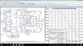
way you don't comment simulation I attached in post #23 instead?
That chart doesn't prove a thing. The slope is 40dB/decade and there's a hodgepodge of poles and zeroes around the ULGF that are (hopefully) bringing the phase back to where it should be for stability. That's not something that any same engineer would do, for anything but a simulation exercise.
You also did not indicate what you represented in the chart (is this the loop gain? if so, an LF open loop gain (as loop gain plus closed loop gain) of ~150dB is yet another insane thing to consider in practice).
You also did not indicate how you modified the closed loop gain, was this by changing the feedback resistor? If so, something is definitely wrong with your simulation, since a 28dB closed loop gain means a feedback resistor x25 the inverting input to the ground resistor. Since the inverting input is loaded by the two resistors in parallel, there's no way the OLG and it's intercept could be modulated by the amount shown, the variation is only about 4%. Anything else could be due to some second order effects, that you don't manage and I don't care about, as long as they are not included in an analytic model.
You pushed me before with this amp, and your claim of stability doesn't tell me diddly squat. As long as you can't explain how your creation is working other than by some global feedback loop simulation, it is in my book nothing but yet another design by simulation, in the absence of any certified device models.
Even so, if it comes to a pure simulation war, I've shown you a pure Lin topology VFA with the same HF double pole and phase correction, with about the same loop gain and ULGF, and about half the number of components. I would not touch a PCB with such an amp with a ten foot pole, though.
Last edited:
Another content-free post. You're getting good at it Waly
Isn't it funny that you are commenting and replying only to my empty content posts? For any other of my posts, I'm probably on your ignore list, where I feel super comfortable. Please keep it this way.
And a current sensing feedback arrangement is just a Howland Current pump, isn't it?
No, not even close.
BTW, nobody called Mr. Jung a salesman. Putting words in other people mouths is a well known fact avoidance tactic.
Last edited:
That's fine. Also that you seemingly don't disagree with the rest of my postNo, not even close.
way you don't comment simulation I attached in post #23 instead?
Dadod, I agree.
Because, Waly can not design audio amplifier using CFA topology, good enough, he think everyone else can not either.
way you don't comment simulation I attached in post #23 instead?
Damir, a PA is designed (usually) for a desired gain depending on your system choices, so it is not fair in this case to simply vary feedback network but re-compensation at each gain must be on the table.
General purpose IC's don't (except in rare cases) have all the necessary handles. What would you have us do, call them all op-amps and tell the customer you figure it out? I almost guarantee taking a basic CFA and converting it to the so-called H-bridge VFA can (if you are allowed to change everything) be configured to be essentially indistinguishable from each other (save input current/noise).
I did this for a customer who wanted for some reason to use very large resistors in the feedback network in an ADSL driver, all distortion/BW specs were easily made.
Last edited:
That chart doesn't prove a thing. The slope is 40dB/decade and there's a hodgepodge of poles and zeroes around the ULGF that are (hopefully) bringing the phase back to where it should be for stability. That's not something that any same engineer would do, for anything but a simulation exercise.
You also did not indicate what you represented in the chart (is this the loop gain? if so, an LF open loop gain (as loop gain plus closed loop gain) of ~150dB is yet another insane thing to consider in practice).
You also did not indicate how you modified the closed loop gain, was this by changing the feedback resistor? If so, something is definitely wrong with your simulation, since a 28dB closed loop gain means a feedback resistor x25 the inverting input to the ground resistor. Since the inverting input is loaded by the two resistors in parallel, there's no way the OLG and it's intercept could be modulated by the amount shown, the variation is only about 4%. Anything else could be due to some second order effects, that you don't manage and I don't care about, as long as they are not included in an analytic model.
You pushed me before with this amp, and your claim of stability doesn't tell me diddly squat. As long as you can't explain how your creation is working other than by some global feedback loop simulation, it is in my book nothing but yet another design by simulation, in the absence of any certified device models.
Even so, if it comes to a pure simulation war, I've shown you a pure Lin topology VFA with the same HF double pole and phase correction, with about the same loop gain and ULGF, and about half the number of components. I would not touch a PCB with such an amp with a ten foot pole, though.
I presented that simulation to show how, I will repeat again, this your statement is not correct:
"- Mr. Jung talks about the "relative constant closed loop bandwidth, regardless of the closed loop gain" which is again correct, but is once again the property of a particular circuit topology (which could be also called "diamond buffer input stage topology" instead of "CFA", but which would be of course way to complex for the marketing departments). It would be also correct and relevant to add "for a certain range of closed loop bandwidths". The property holds indeed for closed loop gains of, say, 0...12dB but no longer holds significantly for closed loop gains of, say, 30...40dB."
I attached full schematic now I used in previous simulation, IPS uses active load (current mirrors) instead resistive load to show how relative constant closed loop bandwidth, regardless of the closed loop gain holds even for closed loop gains of 30..40dB. That was simulated in my previous post. It was Loop Gain of course.
I did not build this amp, just version with resistive load, where the LP is around 80dB, not insane high as you said, and that amp was built in some quantity by different people here from this forum with no stability problem and as some of them said with excellent sound.
In my opinion even that amp with insane open loop gain will be stable in real life, but I decided I don't need to complicate to much to get good CFA power amp.
By the way I don't care any more if you don't care!
Sorry I did not read Scott post before I sent mine. This amp was designed foe 28dB of CLG.
Attachments
Last edited:
Because, Waly can not design audio amplifier using CFA topology, good enough, he think everyone else can not either.
I would not think highly of those that can not do both.
I presented that simulation to show how, I will repeat again, this your statement is not correct:
"- Mr. Jung talks about the "relative constant closed loop bandwidth, regardless of the closed loop gain" which is again correct, but is once again the property of a particular circuit topology (which could be also called "diamond buffer input stage topology" instead of "CFA", but which would be of course way to complex for the marketing departments). It would be also correct and relevant to add "for a certain range of closed loop bandwidths". The property holds indeed for closed loop gains of, say, 0...12dB but no longer holds significantly for closed loop gains of, say, 30...40dB."
It is correct, as you can easily verify on an elementary example (like a CFA opamp). Mr. Wurcer just explained where you are fudging the stuff (me never thought about).
I would not think highly of those that can not do both.
Jesus Christ Allin, the yankee late incarnation of John Simon Ritchie.
Sorry I did not read Scott post before I sent mine. This amp was designed foe 28dB of CLG.
Putting aside the bickering for a moment, let's accept my conjecture that into a load with zero imaginary component one could make a VFA and CFA with the same GBW/slew rate/THD etc. Is there anything different when driving a very difficult frequency dependent load?
Jesus Christ Allin, the yankee late incarnation of John Simon Ritchie.
We had this discussion last night, do you ruin your child's life by giving them a name like Moonshot, Kandy, Cherry, Revilo Oliver?
CFA vs VFA
Short version:
I think it's important to understand that a VFA is a buffered CFA. In a VFA it's not the voltage at the base of the transistor in the feedback loop that is interesting, but the different currents at the "meeting point". In a CFA you dont use a transistor in the feedback loop, but use the current in the feedback loop directly. A so called "Diamont ips" in a CFA can easily be converted to a VFA by buffering the voltage in the feedback loop by another "Diamond" and inserting a Rg between them, a so called H-Bridge. This is my prefered circuit for Audio Amps.
Cheers
S
- Home
- Amplifiers
- Solid State
- Current Feedback Amplifiers, not only a semantic problem?