Greetings to everyone,
as some of you already known, I have in the past tried solutions that could make the V-fet amplifier circuits simpler. Especially I want to remember that on this forum I presented the circuits of the BabySit series which in the simplest version use a single mono power supply. As some already known, V-fet, similarly to tubes, need a polarity of Gate voltage opposite to Drain.
But, meanwhile with tubes it is often possible to use autobias with series cathode resistance, this practice is almost impossible to use with the V-fet due to the large signal losses needed and a consistent increase in output resistance of circuit in relation to the load resistance, with a value comparable to the latter. This problem is not so much felt in the follower schematic, with source output, where it typically needs a single dual voltage, but if you try to use a common source scheme with Drain output, if you want to avoid unacceptable performance losses, to properly polarize the devices, it is really necessary to have 4 power supplies (with few exceptions).
One of these exceptions is to use a Transnova scheme and myself in the past have presented some project with this solution, but I must confess that they have received (wrongly in my opinion) little consideration.
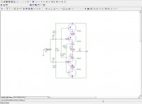
Now, I have developed two new complementary push-pull output circuits, designed for V-fet applications and all other Depletion types as SIT, and Depletion MOSFET, which, although configured as common source amplifiers, they need only one dual power supply and not four different power sources.
I think a lot of simplification for using these devices.
For now I attach the two principle schemes used and then follow some simulations I think interesting.
I obviously look at your considerations on this and good V-fet amplifier at all.
Francesco
as some of you already known, I have in the past tried solutions that could make the V-fet amplifier circuits simpler. Especially I want to remember that on this forum I presented the circuits of the BabySit series which in the simplest version use a single mono power supply. As some already known, V-fet, similarly to tubes, need a polarity of Gate voltage opposite to Drain.
But, meanwhile with tubes it is often possible to use autobias with series cathode resistance, this practice is almost impossible to use with the V-fet due to the large signal losses needed and a consistent increase in output resistance of circuit in relation to the load resistance, with a value comparable to the latter. This problem is not so much felt in the follower schematic, with source output, where it typically needs a single dual voltage, but if you try to use a common source scheme with Drain output, if you want to avoid unacceptable performance losses, to properly polarize the devices, it is really necessary to have 4 power supplies (with few exceptions).
One of these exceptions is to use a Transnova scheme and myself in the past have presented some project with this solution, but I must confess that they have received (wrongly in my opinion) little consideration.
Now, I have developed two new complementary push-pull output circuits, designed for V-fet applications and all other Depletion types as SIT, and Depletion MOSFET, which, although configured as common source amplifiers, they need only one dual power supply and not four different power sources.
I think a lot of simplification for using these devices.
For now I attach the two principle schemes used and then follow some simulations I think interesting.
I obviously look at your considerations on this and good V-fet amplifier at all.
Francesco
Attachments
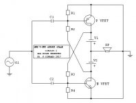
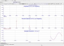
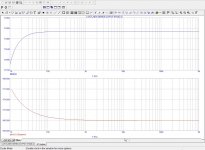
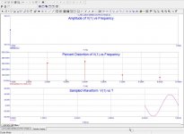
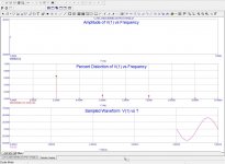
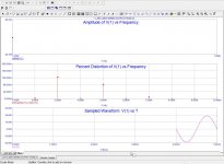
Okay, i will begin with analysis relative to circuit 1. Please note that this is simulated in class AB condition.
Here I post images for:
1)schematic with voltage node in static condition;
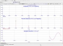
2)Distortion Analysis at 1 W;
3)Relative Distortion numeric value at 1 W;
4)Distortion Analysis at 10 W;
5) " " " 20 W;
6) " " " 30 W;
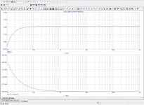
7)Frequency " and Voltage Gain on 8 Ohm load.
P.S.:Not take too seriously this last FR analysis because model of Vfet not contain parasitic caps. It is here to show the GAIN stage in particular.
Here I post images for:
1)schematic with voltage node in static condition;
2)Distortion Analysis at 1 W;
3)Relative Distortion numeric value at 1 W;
4)Distortion Analysis at 10 W;
5) " " " 20 W;
6) " " " 30 W;
7)Frequency " and Voltage Gain on 8 Ohm load.
P.S.:Not take too seriously this last FR analysis because model of Vfet not contain parasitic caps. It is here to show the GAIN stage in particular.
Attachments
-
 V-fet_New_Output_Stage_Analysis_Frequency_Gain.jpg188.1 KB · Views: 186
 -
 V-fet_New_Output_Stage_Analysis_Distortion_30W.jpg159.1 KB · Views: 145
 -
 V-fet_New_Output_Stage_Analysis_Distortion_20W.jpg160.2 KB · Views: 180
 -
 V-fet_New_Output_Stage_Analysis_Distortion_10W.jpg159.7 KB · Views: 189
 -
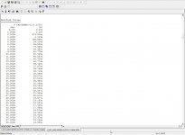
 V-fet_New_Output_Stage_Numeric Dist_Analysis_1W.jpg97.5 KB · Views: 698
 -
 V-fet_New_Output_Stage_Analysis_Distortion_1W.jpg160.6 KB · Views: 753
 -
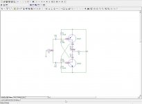 V-fet_New_Output_Stage_Schematic.jpg66.7 KB · Views: 772
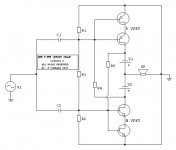
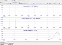
Here in the following simulation about circuit 2. Also this is a class AB amplifier.
Images are related to:
1) scheme with node voltage
2) distortion components at 1 W
3) numeric value of harmonic distortion at 1W
4) distortion components at 10 W
5) distortion components at 50 W
6) distortion components at 100 W
7) distortion components at 200 W
8) frequency response (in limited sense as above) and Voltage Gain.
Attachments
-
 V-fet_New_Series_Output_Frequency_Gain_Analysis.jpg190 KB · Views: 133
 -
 V-fet_New_Series_Output_Dist_Analysis_200W.jpg136.3 KB · Views: 114
 -
 V-fet_New_Series_Output_Dist_Analysis_100W.jpg135 KB · Views: 93
 -
 V-fet_New_Series_Output_Dist_Analysis_50W.jpg137.5 KB · Views: 96
 -
 V-fet_New_Series_Output_Dist_Analysis_10W.jpg135.5 KB · Views: 94
 -
 V-fet_New_Series_Output_Numeric_Dist_Analysis_1W.jpg94.8 KB · Views: 109
 -
 V-fet_New_Series_Output_Distortion_Analysis_1W.jpg160.2 KB · Views: 243
 -
 V-fet_New_Series_Output_Stage_Schematic.jpg74.7 KB · Views: 253
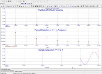
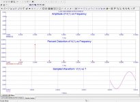
Here in the following simulation about circuit 2. Also this is a class AB amplifier.
Images are related to:
1) scheme with node voltage
2) distortion components at 1 W
3) numeric value of harmonic distortion at 1W
4) distortion components at 10 W
5) distortion components at 50 W
6) distortion components at 100 W
7) distortion components at 200 W
8) frequency response (in limited sense as above) and Voltage Gain.
Thanks mos57 for the node voltages and the interesting sim results. I was curious and connected two SJDP120R085 power depletion FETs [stand alone] like you've connected the 2SK82s. The Vds of the bottom R085 was ~1 V at 1.3A , while the Vds of the top R085 was 20 Vds at 1.3 A. This behaviour appeared like shown in your schematic. Please explain the value of using a pair of [2SK82s] in your schematic versus using one only.
Both schematics show the use of overal negative feedback to each gate plus the interesting biasing scheme in each amp. Is this considered Schade-style negative feedback? if yes will it it augment the inherent triode character of the VFETs and/or alter them.
Thanks.
One of these exceptions is to use a Transnova scheme and myself in the past have presented some project with this solution, but I must confess that they have received (wrongly in my opinion) little consideration.
Hi mos57. Please find attached this interesting article by Jim Stricland inventor of Transova.
Attachments
Thanks for sharing - I hadn't seen that one before!

There is also this at LinearAudio:
https://linearaudio.net/article-detail/2224
Unfortunately not free, but nevertheless, interesting reading on transnova-like designs. I think there is some discussion on it around here somewhere ...
mlloyd1
There is also this at LinearAudio:
https://linearaudio.net/article-detail/2224
Unfortunately not free, but nevertheless, interesting reading on transnova-like designs. I think there is some discussion on it around here somewhere ...
mlloyd1
Hi mos57. Please find attached this interesting article by Jim Stricland inventor of Transova.
Thanks mos57 for the node voltages and the interesting sim results. I was curious and connected two SJDP120R085 power depletion FETs [stand alone] like you've connected the 2SK82s. The Vds of the bottom R085 was ~1 V at 1.3A , while the Vds of the top R085 was 20 Vds at 1.3 A. This behaviour appeared like shown in your schematic. Please explain the value of using a pair of [2SK82s] in your schematic versus using one only.
Both schematics show the use of overal negative feedback to each gate plus the interesting biasing scheme in each amp. Is this considered Schade-style negative feedback? if yes will it it augment the inherent triode character of the VFETs and/or alter them.
Thanks.
Hi Antoniel, if you only measure 1volt of VDS on your R085, unfortunately I think you just add a bunch of distortion.
For the R085 at the bottom you have to select the one with the lowest Vgso, in order to better split the VDS voltages of the two devices.
In actual realization, even in my scheme, I think I will use the 2 external Vfet with the lowest Vgs voltage and the two internal ones with the highest Vgso to allow a better distribution of voltages.
The reason for using two series devices is because the voltage gain is almost double, as shown by the attached results.
One second reason is that it seems to me that with two series devices, although this may seem counterintuitive, the higher order distortions seem to decrease, especially the 5th harmonic (this in the range of 1 to 10 watts) but I need more evidence to be definitely safe.
To answer the last question, I claim to have not sought either the Schade effect or the negative reaction, because my intention is to maximize the stadium gain. For this reason, I would have thought of using CCS in the future instead of simple resistances, but you also have to check the impact this modification might have on sound.

Thanks much for your document.
Last edited:
Thanks for sharing - I hadn't seen that one before!
There is also this at LinearAudio:
https://linearaudio.net/article-detail/2224
Unfortunately not free, but nevertheless, interesting reading on transnova-like designs. I think there is some discussion on it around here somewhere ...
mlloyd1
Thank you very much, very kind.

Regarding the Transnova circuitry and similarities to the circuit proposed here, I hope to shortly prepare an intuitive principle scheme to show how the audio currents go around the two circuits.
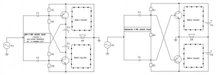
No.
Transnova concept is not follower - in this application, the output mosfets (lateral mosfets, originally sourced by Hitachi) have greater than x1 voltage gain as well as current gain.
This allows driving by a relatively low voltage swing (with hopefully, higher quality/performance) driver circuit, letting the output mosfets do all the "heavy lifting", voltage and current wise.
The link I posted earlier was to an article written by some folks who even used high quality opamps as the driver stage!
mos57 will comment on his own design.
mlloyd1
Hi, both circuits are source followers?
Hello mos57. Should'nt the arrows [for current] run in opposite rather than the same direction. As shown. the amp is pushing OR pulling but not pushing AND pulling.Hi, I drew side by side my scheme and the transnova for a simpler comparison with the indication of the audio currents as they flow in the two circuits.
I look forward to your considerations.
Hello mos57. Should'nt the arrows [for current] run in opposite rather than the same direction. As shown. the amp is pushing OR pulling but not pushing AND pulling.
Hi Antoniel, the lines of the currents are correctly indicated (imho).
This is because they are related to the signal currents and not to the DC current of polarization, which, on the contrary, must be opposed, because there must be no continuous component on the load.
So if also the alternating signal components in the load were also opposed, you would not have any useful signal for your speakers. This applies to both class AB and class A pure and clearly not only for the example circuits but also for all types of circuits that are called push-pull type.
Take two workers who have in their hands a two-hand saw with which they have to cut a piece of wood. Imagine that one is on the right and the other on the left.
We analyze the movements in two:
1) left pushes forward (push) and simultaneously the right pulls back (pull): the saw moves from Sx to Dx.
Stop for a moment to reflect and observe that although the movements of the two workers are opposed, the direction of the saw movement is concordant and it moves in a very precise direction.
What happens in the next is less important: if it had enough length this unique sense of movement (from Sx to Dx), it would suffice to cut all the wood.
But since the blade length is limited, they have to reverse the reciprocal movements (2° stage), or remove the blade and reposition it in the initial condition, but this is another story.
Having said this classic storyline, let's go back to our example and replace the actions of the arms of the two workers (one pushing, the other pulling) with tensions, and replace the motion imprinted on the blade (from Sx to Dx) with our current . At this point it becomes clear that despite voltage appear to have opposite verses (push-pulls), the currents are in agreement.
In other words: if I say that the positive voltage is DIMINING and the Negative voltage is INCREASING (that is, it becomes more negative), it means that the charges are moving all in the same direction (equal direction) to a lower absolute potential.

Thank you mos57 for your explanation of push-pull. My understanding of push-pull came from Google, YouTube and education books which present alternate views as follolws. Current flowing in one direction through a loudspeaker [at its red terminal] facing me pushes its cone towards me [out], and current flowing through the loudspeaker in the opposite direction pulls its cone away from me [in].
The TransNova power output stage is versatile. It simultaneously provides signals for overall negative feedback [like you showed] and for positive current feedback [PCF]. I've used the TransNova methodology and this dual benefit to assemble prototype amps as shown in my thread found in the Pass Labs Forum which is entitled "Amps with simulated/fake SITs" . Great sounding prototypes.
I'll continue to visit your site which has a lot of knowledge and know-how to offer.
Best
i've heard a 9500 playing into some Soundlabs and REALLY liked what i heard!
so, i've always wondered about the comments (many i've seen here) from people who say the Transnova amp sounds funny to them.
to each his/her own (as usual) i guess ...
i do still wonder why you don't see/hear more about transnova clones around here in diyland.
mlloyd1
so, i've always wondered about the comments (many i've seen here) from people who say the Transnova amp sounds funny to them.
to each his/her own (as usual) i guess ...
i do still wonder why you don't see/hear more about transnova clones around here in diyland.
mlloyd1
i do still wonder why you don't see/hear more about transnova clones around here in diyland.
+1
- Home
- Amplifiers
- Solid State
- New V-fet complementary output stage