It uses base charge pull-out of the output rransistors similar to Dimitri Danyuk's Figure 4a and Figure 5 at his Articles folder here, or download PDF. But I haven't seen this specific design before, although I wish I had
 .
.Your post #5 on the link above mentions the clever part,
"... the clever bit, Q23 & Q26: they provide a clean and fast turnoff path to the OP devices, which must boost the HF performances significantly"
Notice output transistors Q28,29 have high impedance (current drive) nodes from Q9,Q25 for Q28, and then Q20,Q22 for Q27. And the bases of the output transistors have a path to pull out base current for fast turn off! Nifty indeed. As well as Class-AB biasing via Q26,Q23 couples bases.
.This could be a solution to speed up the output stage of my CSD amp in Linear Audio Vol.13.
But a transformation is needed from this common collector output stage to apply it to my common emitter output stage.
Alternatively, simply replace my output stage with this output stage. It has a voltage gain set by 1+ R16/R17 or a gain of 4 times. Not enough to directly connect direct to my CMOS input stage, but if the gain is set higher at 10 times (R16 470R) then it might solve our problem of HF distortion and cross-conduction.
I won't simulate it just yet. I'll wait to hear from other's.
Well spotted Elvee!
Last edited:
Is it really cross-conduction?
Hi,
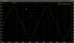
So why is the distortion most apparent on positive to negative transitions of the output voltage? I assume that the fT of both output transistors is approximately the same.
At first guess I would have expected to see similar distortion on the negative to positive transition, assuming the output circuitry is symmetrical.
Regards ....
This delay in switching off is what causes the cross-conduction that Ian referred to.
Hi,
So why is the distortion most apparent on positive to negative transitions of the output voltage? I assume that the fT of both output transistors is approximately the same.
At first guess I would have expected to see similar distortion on the negative to positive transition, assuming the output circuitry is symmetrical.
Regards ....
The problem is not merely slow switching. Now that the drivers control the switching, the output transistors must respond instantly to what the drivers do, otherwise the switching lags after the 0 cross point. The output transistor bases are shunted by both Cbc and Cbe, which amounts to a heck of a lot of capacitance, especially after Miller effect.
We can't compensate for this merely by designing phase lead into the drivers, because part of the charge current is Vout-dependent, and the other part is Iout-dependent. If the load impedance changes, the proportion of charge currents changes and the compensation will be over or under what is needed. And then there is the fact that these capacitances are constantly changing. But maybe compensating the majority of the charge current would be "good enough"?
We can't compensate for this merely by designing phase lead into the drivers, because part of the charge current is Vout-dependent, and the other part is Iout-dependent. If the load impedance changes, the proportion of charge currents changes and the compensation will be over or under what is needed. And then there is the fact that these capacitances are constantly changing. But maybe compensating the majority of the charge current would be "good enough"?
I wanted to see what would happen if I just compensated the Cbc with a known accurate method. This does okay with 12mA keep-on bias provided by I2.
G3 and G4 act as current mirrors, which reference the Cbc currents of Q7 and Q8 to drive the Cbc of Q1 and Q2. This way Cbc is eliminated from the causes of phase shift between the collectors of the drivers and the collectors of the output BJTs.
I don't think anyone will be enthusiastic about the idea of adding expensive BJTs as vegetative limbs, but if you have 5 pairs of BJTs, and use 5x current mirrors, it might have more practical value.
As a proof of concept, it's at least better than before. The asymmetry at crossover is a result of the nonlinear base charge resulting from the exponential Vbe waveform in parallel with Cbe. There are some methods of compensating this as well, but parts count might become exponential.
Attachments
Interesting. Thinking outside the box -- I like that... This does okay with 12mA keep-on bias provided by I2.
What happens if you also add a 12mA keep-on bias for Q7,Q8 'vegetative limbs'?
Also, could you find THD at 1kHz and 20kHz at say half output swing into 8R?
THD is 0.11% at 20k and 1k.
I could bias the vegetables, but I've never found a reason to, unless you go the whole hog and use it as a power device to compensate not just the charge currents but the DC base currents as well. Which gets complex very fast with not much actual practical gain. And in this case, doing so would require the slave BJTs to be voltage driven.
The only way to get that to work would be to give the output BJTs their own feedback loops as power current multipliers, which could have been done in the first place, but the whole point of this exercise is to improve economy and simplicity, no?
Last edited:
With delicate tweaks to the driver degeneration, I can get THD down to 0.014% at 1k and 0.042% at 20k.
The main improvement comes from removing the 2nd harmonic with driver degeneration offset, and finding the Oliver null point for them. It probably is very dependent on load and output voltage, and wouldn't hold up under thermal cycling.
The main improvement comes from removing the 2nd harmonic with driver degeneration offset, and finding the Oliver null point for them. It probably is very dependent on load and output voltage, and wouldn't hold up under thermal cycling.
Attachments
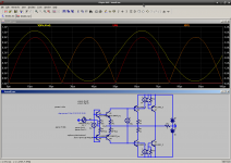
Query about your simulation schematic?
Hi Mooley, When I compare you simulation schematic to the original schematic provided in EW there is a difference. You have both of the 1nf capacitors linked to the output node. Shouldn't Cf be connected to the base of Tr9?
Using BC550, BC560, BD139, BD140, MJE15032 and MJE15033 Cordell models seems to work. With a 20 kHz tone input generating a 30W output the simulation calculates 0.14% THD.
To set the bias to 100 ma required R7 to be increased to 1K (Depends upon hFE values). This can be checked using the simplified equations provided in the original EW article.
Curious, I just simulated the original and find I can not meet the original specs. In fact distortion is pretty obvious in the sim without even looking at FFT's or number crunching. It also seems very transistor (model) dependent.
Hi Mooley, When I compare you simulation schematic to the original schematic provided in EW there is a difference. You have both of the 1nf capacitors linked to the output node. Shouldn't Cf be connected to the base of Tr9?
Using BC550, BC560, BD139, BD140, MJE15032 and MJE15033 Cordell models seems to work. With a 20 kHz tone input generating a 30W output the simulation calculates 0.14% THD.
To set the bias to 100 ma required R7 to be increased to 1K (Depends upon hFE values). This can be checked using the simplified equations provided in the original EW article.
I haven't got the time to read all about this topic, but I'm going to tell you about my experiments regarding this.
For some months ago I "developed" a conceptual amplifier here on diyaudio and I called it the Godzilla amplifier. No one really cared, but I came up with some interesting stuff.
That particular amp had a current driven output stage ( BJT class AB ). But my simulator reported that the THD spectrum differed compared with voltage drive.
Especially h3 was heavily boosted. At around 50 ohm it started and stabilized at 1komh or so. It was a dramatic increase( a factor of ten, worst case). Also h3 was elevated but that came mainly from the different beta between the PNP and NPN devices.
h4 and upward was not affected much.
I thought it was strange so I measured on the real things and that supported the simulation.
This "current drive" circuit is not directly relevant to this thread. But thank's for mentioning it to us. I'll explain why.That particular amp had a current driven output stage ( BJT class AB ).
Your circuit has a bias voltage tying the two bases of the output transistors together which means they are still sensitive to junction temperature changes and still needs a Vbe multiplier to stabilise the bias current.
The circuit in the Linear Audio Vol.13 Current Source Driven amp, and the one by Wim de Jager (mentioned in earlier posts), are free from junction temperature variations upsetting optimum bias. They are quite different output stages to yours.
However, if you read the first post of this thread, you will learn these new stages suffer from the slow turn-off of the power transistors causing HF cross-conduction distortion and extra no load dissipation. Your current drive output stage does not suffer from these problems because the base charge is pulled out via the bias voltage source.
I don't want to discourage you from trying unconventional ideas. There's still unexplored areas like current drive to overcome the age-old problem of how to overcome junction temperature changes affecting optimum bias and thermal runaway (current hogging) with parallel transistors. And the Linear Audio Vol.13 amp has overcome both of these.
Peter Baxandal wrote chapter 2 in the 'Audio Engineer's Handbook' edited by Michael Talbot-Smith and he explains the standard push-pull emitter follower output stage has 3 modes depending on frequency and one of these is current drive. Bob Cordell's design approach is to minimise the current drive region by adding an extra 3rd Darlington stage 'Triple'. This means the current loading on the VAS by the output stage is negligible -- in other words the output stage is voltage driven and not current driven.
In a current driven output stage all the current from the VAS goes into the output stage. In voltage drive none of the current from the VAS goes into the output stage and the VAS current goes into the CCS and the VAS output resistance (due to Early effect) and the Miller compensation capacitor.
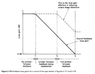
I'll attach the plot by Peter Baxandall showing the 3 regions for the standard Lin topology. This applies when the VAS has a high resistance load (either a CCS or bootstrapping) which is usually the case, but does not apply to the triple Darlington variant.
Peter Baxandall says up to f1 (LF) the output stage is effectively current driven. After f3 (HF) the output stage is voltage driven due to the low output impedance of the VAS from VAS local feedback. Between f1 and f2 there is a transition from current drive to voltage drive. This is probably news to most designers, even well-read ones.
Douglas Self may have explained this in his later Edition's, but I can't quote chapter and verse. Maybe someone can let us know if it's in one of his books.
If you want to read the full text by Peter Baxandall, it's on myDrive here.
Attachments
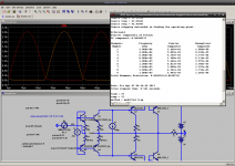
Some more information about simulating Wim's amp
Using the original component nomenclature from the EW article the simulation results when Cf is connected to the collector of Tr9 generates the artifact you are seeing. The biasing has been tuned to 100 ma with 20 KHz sine input. (See attachment MooleyAmp.png)
Using the original schematic with Cf connected to the emitter of Tr8 gives a better result with 100ma bias and 20 KHz sine input. (See attachment WimsAmp.png)
The original schematic set R7 to 150 ohms to give 100ma bias. With the devices I used it was necessary to set R7 to 1K to achieve the same 100 ma bias. The output transistors did have different beta values. This explains some of the asymmetry in the current waveform though the output transistors. Depletion charge also has some effect.
The open-loop bandwidth is less than 1 kHz. I believe this is the main reason the THD is about an order of magnitude worse at 20 KHz compared to 1 kHz. Of coarse it is possible to modify the amplifier schematic and test this assumption.
The artifact that you are seeing is a result of your (unintentional) modification to the original schematic.In fact distortion is pretty obvious in the sim without even looking at FFT's or number crunching.
Using the original component nomenclature from the EW article the simulation results when Cf is connected to the collector of Tr9 generates the artifact you are seeing. The biasing has been tuned to 100 ma with 20 KHz sine input. (See attachment MooleyAmp.png)
Using the original schematic with Cf connected to the emitter of Tr8 gives a better result with 100ma bias and 20 KHz sine input. (See attachment WimsAmp.png)
The original schematic set R7 to 150 ohms to give 100ma bias. With the devices I used it was necessary to set R7 to 1K to achieve the same 100 ma bias. The output transistors did have different beta values. This explains some of the asymmetry in the current waveform though the output transistors. Depletion charge also has some effect.
The open-loop bandwidth is less than 1 kHz. I believe this is the main reason the THD is about an order of magnitude worse at 20 KHz compared to 1 kHz. Of coarse it is possible to modify the amplifier schematic and test this assumption.
Attachments
Thanks for this Ian.I'll attach the plot by Peter Baxandall showing the 3 regions for the standard Lin topology. This applies when the VAS has a high resistance load (either a CCS or bootstrapping) which is usually the case, but does not apply to the triple Darlington variant.
Peter Baxandall says up to f1 (LF) the output stage is effectively current driven. After f3 (HF) the output stage is voltage driven due to the low output impedance of the VAS from VAS local feedback. Between f1 and f2 there is a transition from current drive to voltage drive. This is probably news to most designers, even well-read ones.
Douglas Self may have explained this in his later Edition's, but I can't quote chapter and verse. Maybe someone can let us know if it's in one of his books.
If you want to read the full text by Peter Baxandall, it's on myDrive here.
Great Guru Baxandall tried to school this grasshopper on this arcane subject via some private correspondence in da late 70's.
He used a slightly different hand drawn pic.
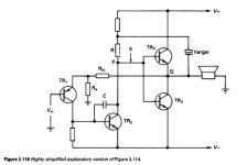
I prefer to maximise the current drive region by adopting pure Cherry compensation.Bob Cordell's design approach is to minimise the current drive region by adding an extra 3rd Darlington stage 'Triple'.
Apart from MUCH better THD20k, this is also MUCH less critical of Iq
Last edited:
The artifact that you are seeing is a result of your (unintentional) modification to the original schematic.
...
Using the original schematic with Cf connected to the emitter of Tr8 gives a better result with 100ma bias and 20 KHz sine input. (See attachment WimsAmp.png)
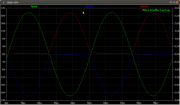
Nice work guys. Thanks for getting it simulating with accessible models.
We can see the slow turn off tail that causes the increase in distortion at 20kHz (your RHS plot).
Any chance of posting the corrected simulation circuit with models?
Any ideas on how to reduce this distortion at 20kHz for Wim's circuit?
Thanks for a very exhaustive reply.
Perhaps I should shut up now since I'm not properly informed in the subject. But if I get it right, the point with Wim's circuit is mainly to increase thermal stability?
I can actually see other benefits such a higher OLG bandwidth which increases the phase margin. Though, I haven't seen that topology in practical designs.
OK, for me the bias stabilizing is a non issue. Self explains his findings about the optimum bias is around 20 to 30 mA per BJT pair. But there is no consensus about that - from a subjective point of view. Personally I prefer around 300mA( if the fins allow it), it gives an impression of "solidity" to the presentation. 300mA actually makes an amp operate in class A up to a quite loud volume ( with normal speakers and room ).
My own Godzilla experiments was really a searching for a very simple solution that only had two stages. A BJT version of the usual Nelson Pass philosophy when it comes to minimalism.
I have made a more domesticated version that works well in real life - I call it "The baby Godzilla". But that one sounds so good that I hesitate to show it here on diyaudio.
Perhaps Wim's circuit is just there to illuminate the operation, but it has some obvious peculiarities. The 1n over Tr8 will make the rails have a huge impact at frequencies where that cap begins to conduct. And when it does, it is affected by that h3 boost I mentioned.
Well, only my thoughts, I don't expect you to spend any time with this issue anymore.
Revised Mooley Simulation
The original EW article points out that the bias current does increase as the device temperatures increase.
The amplifier uses an inclusive single-pole Miller compensation. I want to investigate a 2-pole scheme and see if it possible to effectively reduce the THD at higher frequencies. This is a simple cheap-shot.
Simulating various bias currents shows that increasing the bias current does reduce the THD.
The amplifier uses a geometric-mean bias control. Symmetry is the key. I can't eliminate the effects of charge storage during transistor turn-off. Is it possible modify the circuit to artificially create a mirror effect during transistor turn on?
The simulation of Jager's amplifier is attached. All the semiconductor models are from Cordell. It is running on LTSpice XVII.Any chance of posting the corrected simulation circuit with models?
The original EW article points out that the bias current does increase as the device temperatures increase.
The amplifier uses an inclusive single-pole Miller compensation. I want to investigate a 2-pole scheme and see if it possible to effectively reduce the THD at higher frequencies. This is a simple cheap-shot.
Simulating various bias currents shows that increasing the bias current does reduce the THD.
The amplifier uses a geometric-mean bias control. Symmetry is the key. I can't eliminate the effects of charge storage during transistor turn-off. Is it possible modify the circuit to artificially create a mirror effect during transistor turn on?
Attachments
The simulation of Jager's amplifier is attached.
...
I can't eliminate the effects of charge storage during transistor turn-off. Is it possible modify the circuit to artificially create a mirror effect during transistor turn on?
Hi Tibouchina,
Thanks for making your circuit available. Nice.
I have added a mirror on each power transistor base to pull out base charge based on the rate of change of drive current. I have used temporary voltage sources until I (or anyone) can work out how best to derive the two polarities; one needs to be inverted somehow.
I checked no load at 20kHz and 40kHz. Without the mirrors the average currents in the power transistors doubles at 40kHz. With the mirrors the average current is trimmed to be the same 100mA by varying R12,13; requires 2k2.
Stepping the C value for the mirror capacitor shows the mirror make the gain wobble more at the crossover. I'm not sure if this is what it would do if much faster power transistors were used (much less stored charge) or whether it is the mirror that is hindering the bias loop. More tests are needed to see which it is.
As far as reducing cross-conduction currents this mirror idea works but is tricky to set right and maybe the power transistor junction temperature might upset an optimum setting. Bench tests are needed. Unless the LTspice BJT model has tempco's for charge storage effects, anyone know?
For my Linear audio circuit I tried this mirror idea. I also tried an idea with a mirror linked to 50m ohm emitter resistors for feedback to make it less sensitive to power transistor parameter variations and load variations etc. If you are interested the circuit is available on myDrive here. Sorry it's so messy - I'll tidy it up, sometime, and put all the model stuff in a text file.
Different compensation may get the distortion down to a lower level than at present. Also try MJL3281/1302's which have a higher IKF parameter giving less large signal gain fall which creates mainly 3rd harmonic distortion.
Cheers,
Ian
Attachments
After looking at Jager's circuit in your simulation I can see that Q9 and Q8 perform the switching for the output BJTs, with Q5-Q7 acting basically as a shunt regulator to keep the voltage from Q9's emitter to Q8's base constant. This results in the same switching curve as a normal emitter follower.
Just like the class AB emitter follower it emulates, it theoretically benefits from 26mV emitter degeneration at Q9 and Q8 to smooth out the crossover region and reach the Oliver null point.
This circuit has similar issue with crossover lag as Ian's circuit, but in your simulation the issue is hidden by using faster output BJTs. It seems to work worse than collector drive with Cbc compensation, but better than collector drive without Cbc compensation.
Q6 and Q3 are saturating during normal operation, this needs to be fixed before we can do much about the other parts of the circuit. R8, R3 and R4 are all making saturation worse. Also since Q6 and Q8 operate at 10uA or lower, I suggest using fast small-signal transistors.
Q6 and Q5 have a transfer curve not much different from an ordinary transistor, so the only function performed by Q5 is to reduce the Vbe of Q6 to a useful value for the bias loop. However this also makes them into a very slow, "lazy" shunt regulator. This seems to be causing asymmetry in the crossover points.
Checking a few facts?
1. While there is an excess hole carrier charge the collector current is not zero.
2. When the base current is removed, the excess hole carrier charge decays at a finite rate (governed by a first-order differential equation). During this decay there is an unwanted collector current.
3. You are proposing to quickly remove the excess hole carriers by using a reverse base current? Effectively sucking the charge out of the transistor.
Need to make sure I have the facts straight. Going back to basics for NPN:Hi Tibouchina,
As far as reducing cross-conduction currents this mirror idea works but is tricky to set right and maybe the power transistor junction temperature might upset an optimum setting. Bench tests are needed.
1. While there is an excess hole carrier charge the collector current is not zero.
2. When the base current is removed, the excess hole carrier charge decays at a finite rate (governed by a first-order differential equation). During this decay there is an unwanted collector current.
3. You are proposing to quickly remove the excess hole carriers by using a reverse base current? Effectively sucking the charge out of the transistor.
That's the idea.Need to make sure I have the facts straight.
...
3. You are proposing to quickly remove the excess hole carriers by using a reverse base current? Effectively sucking the charge out of the transistor.
Hi Keantoken,... Q6 and Q8 operate at 10uA or lower, I suggest using fast small-signal transistors.
The attached file has small signal transistors for Q6-8 with Q5 omitted. Also changed to MJL1302/3281. I added a keep-on resistor for 25mA because the loop no longer limits above zero (I don't know why). I set the loop idle current to 100mA (125mA total).
The distortion with frequency is about the same as Wim's amp at 10kHz and 1kHz. Wim used 80MHz power transistors and I have used 40MHztransistors, so we should probably compare his 20kHz THD to our 10kHz THD.
Each power transistor dissipation with no load 2kHz and 20Vpk is 3.1W (125mAx25V). At 20kHz is 4.5W and 6.5W at 40kHz which is about the same as Wim's article. So, not much point in reducing cross conduction dissipation (like the previous mirror circuit). Then how can we reduce distortion at 1kHz and 20kHz?
Cheers
Attachments
- Status
- This old topic is closed. If you want to reopen this topic, contact a moderator using the "Report Post" button.
- Home
- Amplifiers
- Solid State
- Current-Source-Driven-power-transistors-and-mitigating-cross-conduction-distortion