After years of ruminating; I finally knuckled down
and built my first "Blameless" power amp.
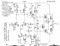
Schematic attached, and some Images attached.
The design philosophy > Build a medium power "Blameless" amp
from 'junk-box' parts and see how it plays.
The design criteria >
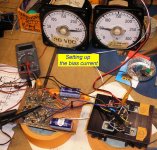
1) 25W output into 8 ohms ( So as not to blow my speakers, again ! )
( Lots easier to replace transistors than to rewind a voice coil !! )
2) Use garden-variety, slow, old fashioned, GP BJT's, just to see
how good an amp can perform with circa 1970's transistors...
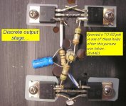
MJE2955/3055 outputs, TIP29/30 drivers MPS A42/92 pre-drivers
and a scattering of the 2N44xx family of NPN and PNP complements.
All antique BJT's , dirt cheap.
And the results ?
In a word, Spectacular !
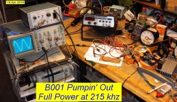
Power Bandwidth 10 - 250khz
Unity gain stable, thermally stable.
A quarter megahertz BW
oughta be fast enough for anyone.
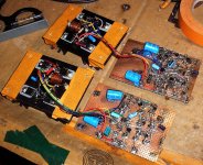
Made a few small design changes from Prof Selfs' published circuit:
( separate current sources for the diff-amp and VAS )
Hand selected the mirror and LTP transistors for Vbe match...
( Quiescent DC offset on the output < 10 mv )
Increased the speed up cap on the output transistors to 22 uf
( this is right in line with my work on mag oscillators where
lots of capacitance in the base drive will transition the device
in less than a microsecond...)
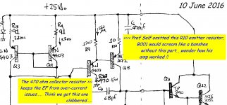
Had a series of Q7 failures, ( the EF between the LTP diff amp
and the VAS ), induced by over-drive, >>> Q7 collector current
was un-restrained.....Now limited by 470 ohms, no more failures.
Also noticed parasitic oscillation when VAS Q8 approached saturation,
selecting thru a pile of MPSA92's reduced the oscillation to a minor annoyance.
Discovered that the VAS needed an emitter resistor,
or else the amp would oscillate like a banshee for any input level.....
10 ohms worked well.
In conclusion >> Overall, a most enjoyable project !
Thundering away here in the bedroom
driving my antique RSL 28's bookshelf speakers !
Don't have equipment to measure THD, or TIM, or Slewing distortion,
still I am really pleased with the sonic performance.
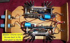
My "B001/B002" pair now in daily use for several months.
Plan to install a Zobel network down the line somewhere,
but for now the amp sounds terrific; good enough for this old coot.....
And yes, I know it can be improved, will do that on the next project,
a "75W Blameless amp"...On the drawing board.
There is no such thing as building too many amplifiers.
and built my first "Blameless" power amp.
Schematic attached, and some Images attached.
The design philosophy > Build a medium power "Blameless" amp
from 'junk-box' parts and see how it plays.
The design criteria >
1) 25W output into 8 ohms ( So as not to blow my speakers, again ! )
( Lots easier to replace transistors than to rewind a voice coil !! )
2) Use garden-variety, slow, old fashioned, GP BJT's, just to see
how good an amp can perform with circa 1970's transistors...
MJE2955/3055 outputs, TIP29/30 drivers MPS A42/92 pre-drivers
and a scattering of the 2N44xx family of NPN and PNP complements.
All antique BJT's , dirt cheap.
And the results ?
In a word, Spectacular !
Power Bandwidth 10 - 250khz
Unity gain stable, thermally stable.
A quarter megahertz BW
oughta be fast enough for anyone.
Made a few small design changes from Prof Selfs' published circuit:
( separate current sources for the diff-amp and VAS )
Hand selected the mirror and LTP transistors for Vbe match...
( Quiescent DC offset on the output < 10 mv )
Increased the speed up cap on the output transistors to 22 uf
( this is right in line with my work on mag oscillators where
lots of capacitance in the base drive will transition the device
in less than a microsecond...)
Had a series of Q7 failures, ( the EF between the LTP diff amp
and the VAS ), induced by over-drive, >>> Q7 collector current
was un-restrained.....Now limited by 470 ohms, no more failures.
Also noticed parasitic oscillation when VAS Q8 approached saturation,
selecting thru a pile of MPSA92's reduced the oscillation to a minor annoyance.
Discovered that the VAS needed an emitter resistor,
or else the amp would oscillate like a banshee for any input level.....
10 ohms worked well.
In conclusion >> Overall, a most enjoyable project !
Thundering away here in the bedroom
driving my antique RSL 28's bookshelf speakers !
Don't have equipment to measure THD, or TIM, or Slewing distortion,
still I am really pleased with the sonic performance.
My "B001/B002" pair now in daily use for several months.
Plan to install a Zobel network down the line somewhere,
but for now the amp sounds terrific; good enough for this old coot.....
And yes, I know it can be improved, will do that on the next project,
a "75W Blameless amp"...On the drawing board.
There is no such thing as building too many amplifiers.
Attachments
")

Q10 substitution ----
Just about any NPN will work for the Vbe multiplier....
as long as it has enough beta>> anything over ~20 will do the job.
Your BDE 139 will probably work fine....bolt it to the heatsink.
( make sure it is insulated !! the BDE139 appears to have
the collector terminal on one side of the package )
In my design I drilled a hole in the midst of the to-220's
and epoxied the TO-92 pak into the hole.
Thermal tracking is excellent....
Years ago, in a Marantz 2215 restoration, I
drilled out the heatsink and expoxied in two
1n914 diodes in the holes.... Thermal tracking
was much improved over the OEM design
where they simply clamped a dual diode pak
to the heatsink surface......
When you finish your Amplifier build,
please post the results so we can all have
a look !
Attachments
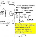
Move the R12 VR to the other side of the Q20 base. At present if the wiper goes momentarily open circuit the bias voltage jumps up to ~4½Vbe. Fortunately not too high since you have selected limiting resistor values.
Better to have it in the BE side and make it a 1k or 2k VR. Reduce R13 to 510r to make the highest bias voltage ~4.9Vbe, if you accidentally leave VR=zero at turn ON.
Add RF attenuation at the input. 1k series and 1nF will be a bit too severe, but you get a ball-park 1us RC to start with. Just parallel across the 1k to reduce the RC in stages, till you find it having no effect on the treble, then go back one step.
Select your highest gain for Q7 to reduce the current injected into the unbalanced LTP. The injected base current has to match the current imbalance of the mirror due to two Ib being fed into the -ve side of the LTP.
R7 & C2 severely limit your low frequency extension and force C2 into becoming a filter. This will create distortion.
C2>sqrt(2)*C1*R1/R7, i.e. >97.5uF. Use 100uF or 150uF or 220uF to minimise the LF distortion and prevent it working as a filter.
If you want to limit the LF from your amp, do it at the input by changing C1. A plastic film cap here works very well if it filters @ ~1decade below your required LF passband.
I don't like the reverse transistor for a Zener. Use a LED, or two, for 1.9V, or 3.8V, of bias for the CCS. A red LED or IR LED instead of the two 1n4148 also works well.
I think you should look at a big increase in R3 & R4. I suggest you aim for 300mVdrop to 1Vdrop across these resistors, 200r works.
I am glad to see you added R16 to protect the VAS helper. D.Self and many others got that wrong.
The big increase in C4 from 2uF to 22uF looks about right.
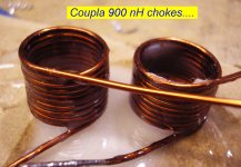
Definitely add at a minimum an output Zobel. Even better to go the whole hog and fit a Thiele output network consisting of the shunting R+C and the series pair of L||R
Try 10nF+8r for the shunt
Try 1uH||4r for the series.
You can optionally fit an extra shunt across the speaker terminals. Try 4r+100nF
The 4r in the series and this extra add up to 8r and give an effective 8r+100nF. The two Zobel now combine to give 4r+200nF.
This extra Zobel at the speaker terminals attenuates RF coming in from the speaker cables.
I like your philosophy of using "old fashioned" devices to see how they work within a good design.
I think you have proved that good design makes the performance almost independent of the device parameters.
Better to have it in the BE side and make it a 1k or 2k VR. Reduce R13 to 510r to make the highest bias voltage ~4.9Vbe, if you accidentally leave VR=zero at turn ON.
Add RF attenuation at the input. 1k series and 1nF will be a bit too severe, but you get a ball-park 1us RC to start with. Just parallel across the 1k to reduce the RC in stages, till you find it having no effect on the treble, then go back one step.
Select your highest gain for Q7 to reduce the current injected into the unbalanced LTP. The injected base current has to match the current imbalance of the mirror due to two Ib being fed into the -ve side of the LTP.
R7 & C2 severely limit your low frequency extension and force C2 into becoming a filter. This will create distortion.
C2>sqrt(2)*C1*R1/R7, i.e. >97.5uF. Use 100uF or 150uF or 220uF to minimise the LF distortion and prevent it working as a filter.
If you want to limit the LF from your amp, do it at the input by changing C1. A plastic film cap here works very well if it filters @ ~1decade below your required LF passband.
I don't like the reverse transistor for a Zener. Use a LED, or two, for 1.9V, or 3.8V, of bias for the CCS. A red LED or IR LED instead of the two 1n4148 also works well.
I think you should look at a big increase in R3 & R4. I suggest you aim for 300mVdrop to 1Vdrop across these resistors, 200r works.
I am glad to see you added R16 to protect the VAS helper. D.Self and many others got that wrong.
The big increase in C4 from 2uF to 22uF looks about right.
Definitely add at a minimum an output Zobel. Even better to go the whole hog and fit a Thiele output network consisting of the shunting R+C and the series pair of L||R
Try 10nF+8r for the shunt
Try 1uH||4r for the series.
You can optionally fit an extra shunt across the speaker terminals. Try 4r+100nF
The 4r in the series and this extra add up to 8r and give an effective 8r+100nF. The two Zobel now combine to give 4r+200nF.
This extra Zobel at the speaker terminals attenuates RF coming in from the speaker cables.
I like your philosophy of using "old fashioned" devices to see how they work within a good design.
I think you have proved that good design makes the performance almost independent of the device parameters.
Last edited:
can i replace Q10 with BD139? just for the purpose of easy mounting..
sure you can...
you have proved that good design makes the performance almost independent of the device parameters.
that has been the goal eversince amp building started...
and with today's improved devices, an easy thing to do...
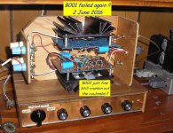
B001 / B002 upgrades ...
Halo Andrew T !
Thank you for your expansive critique.
I am most honored that you would spend
the time to evaluate my pedestrian design effort....
Yeah, the Vbe multiplier >>>> you nailed it !
The pot is on the wrong side of the divider.
I stand corrected ! I will fix it.
On the current mirror, I originally had 220 ohm resistors
for R3/R4, but observed Asymmetrical clipping at full output.
Symmetrical clipping is much more cute;
so after checking DSelfs' comments on mirror resistors,
I dropped the value to give roughly 1/2 Vbe drop.....
... as is, measured quiescent mirror currents
seem to be within 5 percent of each other.
Is that adequate ?
I sure don't know !
Hmmm.... Q7 beta , gonna havta chew on that one for awhile.
Not sure what you are getting at.....But you are probably right.
R7 & C2 >>> okay, missed it again; I stand corrected !!
On the constant current sources, I had considered using an LED
( most enchanting to have little lights embedded with all the tiny parts ! )
but while musing on LED forward drop over temperature...
discovered that LED Delta-V temperature coefficient
is typically 10x compared to a standard PN junction !!
25mv/C vs. 2.5mv/C
and it can be plus or minus ...
Ain't that a kick in the head !!
So with regard to temp stability,
percentage wise the LED loses....
Mebbe oughta stick to the two 1N914's
Which brings up a whole precession of rhetorical questions....
Just how stable do the CCS's need to be ?
The diff amp CCS ostensibly sits at ~6ma.
How much does a reverse NPN drift over temperature ?
What if it were to drift up or down by say,
20 percent over the course of an afternoon?
30 percent ??
Would that drift even matter, and
would amplifier performance be detectably degraded ?
One can only wonder....
Hmmmm........... got lots to think about.
And the outputs.... Yes, the existing topology is profoundly sub-optimal.
I really appreciate the suggestions on component values here !
The reworked Zobel network is in process....
One question >> does the series RC to ground
have to be connected before or after the big output choke ?
Okay that's about it from this end,
Thanks again for taking the time to critique my project...
((There is no such thing as building too many amplifiers.))
All the best,
- ATXmadman
===============================================
" You know how Engineers are,
always changing things"
--- Commander James T Kirk, Starship Enterprise
Attachments
Most think that the first Zobel should be before the output inductor. That is one of the TWO OPTIONS that Neville Thiele gave for the Thiele Network.
N.T. also showed the capacitor after the inductor.
Cherry did a short paper on this explaining that the two extremes given by N.T. are part of a continuum.
Leach uses the alternative.
I look at it slightly differently.
The Zobel is a high frequency load that helps stabilise the output stage. It cannot do this if the inductance around the loop Output-Zobel and back is big. This requires the Zobel to be very close to the output stage and coupled directly to the HF decoupling at the Output stage. It cannot work effectively if one takes the loop out to the PSU, or to the speaker terminals.
8r + 100nF has an F-3dB @ 199kHz. It starts to have a loading effect ~1decade below that. i.e. it is just starting to load the output stage at the very top end of the audio band. It is a heavy load at 200kHz and beyond.
Adding the 4r parallel to the inductor and the 4r + capacitor across the speaker terminals gives a combined 4r+200nF for the same F-3dB@ 199kHz
Now RF interference arriving at the speaker terminals sees two routes
a.) the 4r+100nF as a load between the two wires.
b.) the 4r||inductor in the route to the NFB
a.) shaves off some of the RF before it gets into the NFB.
Last edited:
- Status
- This old topic is closed. If you want to reopen this topic, contact a moderator using the "Report Post" button.
- Home
- Amplifiers
- Solid State
- First shot at the "Blameless" amp topology