After taking those connectors apart and brushing them down with deox-it I've been trouble free with about 15-20 hours of use. Even went in and chopsticked around and no trouble. So the new headers might be a nice add, it seems just a good cleaning can take of the issue. Didn't mean to stress you out!
I've not done the JST pins, but done plenty of similar molex connectors with needle nose pliers and a bit solder with no trouble.
Tim
I've not done the JST pins, but done plenty of similar molex connectors with needle nose pliers and a bit solder with no trouble.
Tim


Me too!
That would have been nice when I purchased minegreat job!
gabo
.
Thanks very much for the offer, but I made my own. Soldering those little pins in was a pain, but persistence prevailed!!
My 565's are awesome and power my stereo/video main speakers. I recently had some friends over to watch a movie and they all commented that the sound was better than at the public theater.
I'm now off building a Baby Huey El34 tube amp, fun project and coming along.
thanks, gabo
Gary and Phil, would you like me to send you some cables? Or did you make your own?
Thanks very much for the offer, but I made my own. Soldering those little pins in was a pain, but persistence prevailed!!
My 565's are awesome and power my stereo/video main speakers. I recently had some friends over to watch a movie and they all commented that the sound was better than at the public theater.
I'm now off building a Baby Huey El34 tube amp, fun project and coming along.
thanks, gabo
Hey Phloodpants. Nice to see you made a small business out of 565 restorations!! I finally got back to my audio projects after 2-3 years of insane workload. Using my shelter-in-place time to finish up my Adcoms and also the Equal Opportunity tube phono preamp.
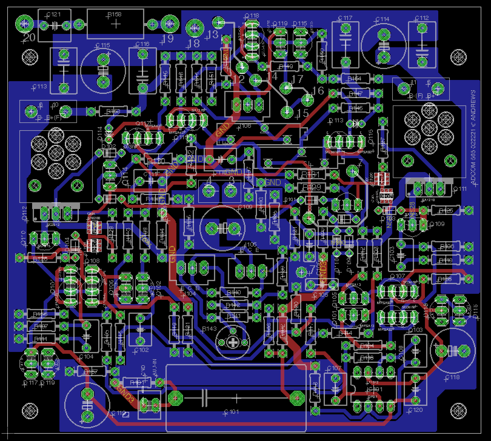
When last we talked I had redone my board (which worked other than the wrong pin position for the heatsinks) to use the CMX SMD devices. This frees up a ton of space on the board in that crowded area around the heatsinks.
Love your approach of facing the devices together and heat shrinking them together for thermal matching. I also see you co-opted the ECBE pinout trick from the matcher. That's a great idea for the board, although I'd have to spend a lot of time redoing my layout to get that squeezed in.
Nice website too!
I'll be posting my new board progress over the next month or so. I have six 565s that I'll be redoing Several of them are operational with a cleaned up original board, but I am going to redo all of them. As you point out the drift over time from the pickled boards can be an issue. If you recall, I had one that I could not get to settle down. It would work one day, and then the next it would be off balance again. That's what drove me to try doing a new board in the first place.
Anyway, I just wanted to say hi, and good work!
Scott
Last edited:
You folks may already be aware of this site, and this article, but I found it interesting. This is written by Nelson Pass, who designed the GFA 555. The 565 uses the same basic cascode architecture.
https://www.passlabs.com/press/cascode-amp-design
https://www.passlabs.com/press/cascode-amp-design
GFA565 output drive resistors open
Working on 565 that was in storage for 10 years. Discovered all output 10 ohm base drive resistors on the PNP side are open. Has anyone seen this? Or have an idea what would cause this? All transistors ohm out okay.
Also working on 2 other amps, replaced 220uf caps and fuse-able resistors washed back side of circuit board with acetone but still have wandering offset.
When cleaning the board how can tell when it’s clean enough?
The problem is that the electrolyte actually soaks into the board, and continues to migrate further into the fiberglass, no matter how well you've cleaned the surface. The only good way to get the original board working properly, is to fly all the high-impedance traces in the input section above the board on solid wires.
Are you speaking of pins 2 & 3 on the IC or the audio input circuit.
Thanks;
Yes, but that's just for starters. The connections to the bases of all 8 transistors in the input stage, the resistors that connect them, and I don't know what else... anything and everything high-impedance. I haven't tried this but I know it can be done. Huge PITA.
I have restored a number of these amps at this point. Some were easy, and some never did settle down. That was the motivation to create a new board.
On the one that would not settle down I would get it working one day, and then come to my lab the next, and it would be all over the place. I finally put my DVM probes right onto the fiberglass of the PCB and measures various voltages on what was supposed to be an insulator! If you are very lucky, you can replace the caps and any blow parts on an existing board (I am about 2 for 3 on this), otherwise you will chase your tail forever. I recommend going with an entirely new PCB. I did my own design, but Phloodpants sells a board and a kit, so go there.
On the one that would not settle down I would get it working one day, and then come to my lab the next, and it would be all over the place. I finally put my DVM probes right onto the fiberglass of the PCB and measures various voltages on what was supposed to be an insulator! If you are very lucky, you can replace the caps and any blow parts on an existing board (I am about 2 for 3 on this), otherwise you will chase your tail forever. I recommend going with an entirely new PCB. I did my own design, but Phloodpants sells a board and a kit, so go there.
Taking advantage of a slow spot in my business to finally finish my revised board. Ordered some, and thew realized, to my dismay, that I had forgotten to include the overload diodes and LED connections! I was able to cancel the order, and spent the afternoon redoing the layout. This one uses the SMD stabistors identified by Chris Hoppe. I have also included high quality Vishay trimmer pot's on the bottom of the board so I can fine tune the input stage current balance instead of relying on resistor stability. I found these to be very useful when troubleshooting these amps, so I figured it might make sense to include them on the board. I may take Chris' advice and move the Zobel network off the board, since it is really not necessary there, and with the trimmers, and the S/MPS transistor option pads, the board is pretty crowded!
I have seven of these amps, and plan to restore all of them, keep three and sell the rest. I'll try to follow Hoppe's level of finish quality (a high bar!!)
I have seven of these amps, and plan to restore all of them, keep three and sell the rest. I'll try to follow Hoppe's level of finish quality (a high bar!!)
Last edited:
Very nicely done. You may get your 6 amps fixed and realize how good they are and decide not to sell them! haha.
If you do get them finished and decide to sell them, I know a recording studio that might be interested in a pair. I built his main monitor speakers for him and when he auditioned them I powered them with my 565s.
gabo
If you do get them finished and decide to sell them, I know a recording studio that might be interested in a pair. I built his main monitor speakers for him and when he auditioned them I powered them with my 565s.
gabo
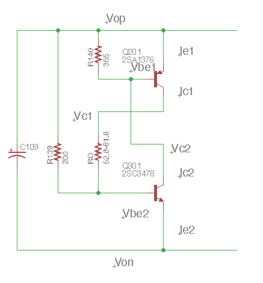
I am trying better understand how the thermal bias compensation network works. It is a cross coupling between the positive and negative signal lines, which are biased slightly positive and negative from ground. This circuit uses the temperature of the two transistor junctions, which are remotely mounted on the power transistor heat sinks, to adjust the offset voltage on the triple Darlington power stages.
Remember from some earlier posts, that the signal to the positive bank is slightly offset positive, and the signal to the negative bank is slightly offset negative (the difference between them is about 3 volts). This means that the positive side starts conducting while the negative side is still conducting, which is the Class A part of the Class A/B operation that makes this aplicfier somewhat unique, especially for a big amplifier.
Here is a simplified schematic that is much easier to follow than the diagram in the manual. The lines labeled Vop and Von are the positive and negative signal lines, but remember here we are not interested in the AC signal, but only the DC component.
Because the two positive and negative signals are in exact phase, this circuit floats between them, and thus is is effectively only operating at DC.
Note that in this diagram, I have bundled R141, R142 and R143 together and call this resistance Ro. That network basically creates a resistance that can be varied from 52.8 ohms to 61.8 ohms.
I plan to dive into this today, and try to better understand how this works. I'll report back soon.
Last edited:
- Home
- Amplifiers
- Solid State
- Yet Another Adcom GFA-565 Thread