Howdy
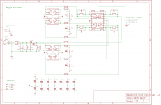
I have been working on a board for Self's "5532 Low Noise Unity Gain Balanced Input Stage" (Fig 18.28 of Small Signal Audio Design 2nd Ed.) but using the lower noise quad LM4562, i.e. the LME49740. Attached is a pic of my circuit (right channel; the left channel is the same obviously).
My circuit incorporates unbalanced input as well. I am aware that there will be a volume mismatch between balanced and unbalanced inputs but this is something I am prepared to live with. (I do not expect inputs to be regularly swapped back and forth between balanced and unbalanced and so any relative volume difference won't be an issue.)
I have a question regarding the grounding of the HF filters etc before the unity gain buffers (U$1 and U$2 in the circuit). The discussion in Chapter 18 of the aforementioned text has each of C1-C2, R3-6 (references to part numbers in my circuit) simply grounded. It seemed sensible to me (a novice) to ground, at least, the HF filters R1/C2 and R2/C1 via Pin 1 / Pin GND on the XLR connector, i.e. directly to chassis, rather than letting any RF enter the circuit (signal) ground. I just continued to ground R3-6 the same way. I am, however, unsure whether this is a sensible approach. Perhaps I can get some "best practice advice" from people here.
I continue to fine tune the board layout/routing, but I have attached a pic of where I have things currently. The board is 5cm x 120cm and the idea is that all the connectors are hard-wired to the board and so support it in place. I have endeavoured to keep signal routing to the top layer where possible and the power for the quad op amps on the bottom layer (each using the other layer only where necessary). I felt a four layer board necessary (well, three layers but it seems that's rare) to get a decent ground plane. Therefore, the middle two layers will be ground planes (not yet added in the board so as to not clutter the pic I have attached). All vias extend through all layers and so vias from top or bottom layer to GND will link both of the middle layers.
If anyone has any constructive comments on the layout I would appreciate that as well.
Thanks in advance!
Steve
PS: I know the LME49740 is 'end of life' and stock from Mouser disappeared over the last couple of days, even while I had some in my basket. However, I have enough for my purposes and in any event perhaps the LMP8674 is a worthy substitute (it seems to have even better noise specs).
Attachments
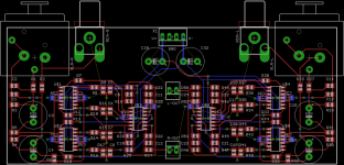
I use KiCad PCB and find that if I route the supplies and grounds manually, this vastly improves the odds that I won't despise the final flooded and filled "planes" after autorouting. I just use min linewidth traces for the hand routed supplies, and let the flood fill make em fat, later.
For example if I connect up all the ground pins with hand routes on the green layer, then when I flood-fill the green layer with ground, I know that there won't be any pins that connect to ground through long meandering traces with one or more vias.
For example if I connect up all the ground pins with hand routes on the green layer, then when I flood-fill the green layer with ground, I know that there won't be any pins that connect to ground through long meandering traces with one or more vias.
@Mark, I can do the same in Eagle but if you look at all the traces in blue (bottom layer) from power and signal traces these slice up any bottom-layer ground plane and hence I thought it better to have a separate ground plane(s) on the internal layers.
@nigel, perhaps you are right but boards are so cheap I was thinking 'play safe'
@derfnofred, I haven't looked at the OPA1612 but a quad saves an enormous amount of board space and routing complexity. There's also op amps such as the AD797 (I have some limited previous experience with this rocket fuelled op amp) and the LT1028. The only quad I have found with specs similar to the venerable LME49740 (LM4562 quad) is the LMP8674 but I have not done a particularly extensive search as I have a bunch of the LME49740.
@dewardh, I started thinking about the THAT products having read the material on Elliot Sound Product's website but was steered heavily away from such implementation as being 'dated' and 'not low noise'. Have you read Self's material? The goal is to get a balanced input stage that has a noise level as good as or better than an unbalanced input.
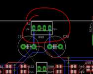
Anyone have a view on my grounding to XLR Pin 1 / GND / Chassis versus to 'regular (signal / circuit) ground' question? (If you look closely at the middle left of the circuit you'll see I have labelled the ground differently, as PE, allowing me to route it separately from GND elsewhere (RCA unbalanced input shield, power GND, GND at voltage dividers ahead of differential amplifiers).)
@nigel, perhaps you are right but boards are so cheap I was thinking 'play safe'
@derfnofred, I haven't looked at the OPA1612 but a quad saves an enormous amount of board space and routing complexity. There's also op amps such as the AD797 (I have some limited previous experience with this rocket fuelled op amp) and the LT1028. The only quad I have found with specs similar to the venerable LME49740 (LM4562 quad) is the LMP8674 but I have not done a particularly extensive search as I have a bunch of the LME49740.
@dewardh, I started thinking about the THAT products having read the material on Elliot Sound Product's website but was steered heavily away from such implementation as being 'dated' and 'not low noise'. Have you read Self's material? The goal is to get a balanced input stage that has a noise level as good as or better than an unbalanced input.
Anyone have a view on my grounding to XLR Pin 1 / GND / Chassis versus to 'regular (signal / circuit) ground' question? (If you look closely at the middle left of the circuit you'll see I have labelled the ground differently, as PE, allowing me to route it separately from GND elsewhere (RCA unbalanced input shield, power GND, GND at voltage dividers ahead of differential amplifiers).)
My circuit incorporates unbalanced input as well.
I think you should make a provision to ground the unused input pin when you use the SE mode.
Through a resistance representing the SE source R expected.
Otherwise you'll muck up the CMRR which, in a SE circuit, really means changing the gain.
jan
Last edited:
Hi Toni. Does that require using two separate power supply entry points (and caps) given 0V is brought to the circuit from the PSU? Presumably it does.
Think if you would build a mono amplifier. Put two of them in one case. Dual mono!
BR, toni
Hi Jan. Interesting suggestion. I was thinking more about grounding the SE input when using balanced as a precaution and was thinking about some sort of jumper terminal where the jumper had to be removed for SE use. But you open up the other side of the coin re SE use... Need to think about how exactly to do that. BTW my intention is to use this with balanced connections but it seemed appropriate to build in provision for SE use.
Hi Jan. Interesting suggestion. I was thinking more about grounding the SE input when using balanced as a precaution and was thinking about some sort of jumper terminal where the jumper had to be removed for SE use. But you open up the other side of the coin re SE use... Need to think about how exactly to do that. BTW my intention is to use this with balanced connections but it seemed appropriate to build in provision for SE use.
Maybe add a small signal relay controlled ground switch if using only se inputs...
Think if you would build a mono amplifier. Put two of them in one case. Dual mono!
BR, toni
Ok will try. I should make it so the board can be snapped into two. Not sure yet how to do that in Eagle / with the board house but I presume I could use some sort of panelisation.
Ok will try. I should make it so the board can be snapped into two. Not sure yet how to do that in Eagle / with the board house but I presume I could use some sort of panelisation.
... maybe design a mono board which can be stacked using distance bolts or so...
Then you are free in your decision to build a multichannel amplifier...
")
Last month I built a PCB that was intended to be snapped into two sub-boards. My Chinese PCB fab does offer that as a service, but I didn't want to pay the $12 extra since the boards were only $16 to begin with. So I just drew a straight line on top and bottom soldermask layers of the PCB layout, 50 mils wide (1.27 mm) and required a clearance of at least 1 mil from the line to all component bodies and all traces on all layers. Then a vise and a Dremel tool with cutoff wheel did the rest, quite easily. It turned out to be simple to keep the cutter completely within the 50 mil wide cut-line, even for someone with not especially steady hands nor excellent eyesight. Then five quick rubs on the sanding block and Bob's your uncle. I wore a dust mask as I prefer not to inhale FR4 dust.
@dewardh, I started thinking about the THAT products having read the material on Elliot Sound Product's website but was steered heavily away from such implementation as being 'dated' and 'not low noise'.
-107dBU unweighted over 20kHz bandwidth seems pretty low noise to me.
http://www.mouser.com/ds/2/407/1200data-542.pdf
-107dBU unweighted over 20kHz bandwidth seems pretty low noise to me.
http://www.mouser.com/ds/2/407/1200data-542.pdf
Self measures the 'quad LM4562 buffer + quad diff amp 820R LM4562' circuit as -119.5dBu - only just less noisy than an unbalanced input by 0.5dB
Hi Jan. Interesting suggestion. I was thinking more about grounding the SE input when using balanced as a precaution and was thinking about some sort of jumper terminal where the jumper had to be removed for SE use. But you open up the other side of the coin re SE use... Need to think about how exactly to do that. BTW my intention is to use this with balanced connections but it seemed appropriate to build in provision for SE use.
At this point, Doug Self's Small Signal Design book becomes invaluable!
Maybe add a small signal relay controlled ground switch if using only se inputs...
Sounds complicated. The circuit would have to automatically detect which input was being used. I was thinking something much more simple. In post 11 I said "grounding" when I meant "open circuit" the SE input when balanced was being used. A simple two position shorting jumper like this would take care of that. Okay it requires the user to open the case and install/remove the jumper but it seems to me the additional complexity of automating it isn't worth it in a DIY setting. I could place a switch on the enclosure but again that seems a pain. In fact, as per the below, Self shows an example of a switchless balanced and SE input board which leaves both inputs connected at all times (but advises users not to leave cables attached to both). The jumper which can, when removed, open-circuit the SE input is an added precaution.
I'm still chewing on Jan's comment. In Small Signal Audio Design chapter 18, Self discusses combined balanced and unbalanced input amplifiers with no switching. My circuit was an attempt to combine this and the ultra low noise design discussed on later pages. (For those with the text, take a look at Fig 18.1, 18.10 and 18.28 - and 18.9.) Perhaps I botched it. I didn't connect the SE input at the unity gain buffer input as might be implied by Fig 18.10 because I would have had to replicate all of the RF filtering and DC blocking components (compare my circuit with Fig 18.1) already present on the pin 2 XLR leg. (Once again, I'm not worried about the volume imbalance between balanced and SE inputs.)
Still no takers on grounding the RF filter etc to chassis through the XLR connector versus to circuit ground?
PS: Toni, circuit now changed to accommodate dual mono / separation of the boards down the middle. I think I can get away without any mounting holes (for stacking or otherwise). The XLR connector can easily hold the board in place. (I will oversize the XLR and RCA solder pads for a bit more security.) A user can use the board in 'stereo' configuration or split boards for use in 'mono' configuration, stacking them however they want.
Last edited:
- Status
- This old topic is closed. If you want to reopen this topic, contact a moderator using the "Report Post" button.
- Home
- Amplifiers
- Solid State
- Self's "5532 Low Noise Unity Gain Balanced Input Stage"