Bad news, my scope gave up the ghost. Not sure I can be much help now. There will be no way to verify anything without it. Looks like I have a big investment to make.
What's wrong with your scope? Scope repairs might be a cool project.
The CRT and Flyback aren't screwed then. Drain the high voltage to the CRT and look for crispy parts or leaky caps first. There are quite a few people here that can help with this. I'm in the middle of repairing an old Daytona arcade game CRT display. Neat old technology!
The traces are super thick.
Have you try to adjust Focus ?
I hope it just cold solder of trimpot or leaky Capacitor
The CRT and Flyback aren't screwed then. Drain the high voltage to the CRT and look for crispy parts or leaky caps first. There are quite a few people here that can help with this. I'm in the middle of repairing an old Daytona arcade game CRT display. Neat old technology!
Did I say ghost? All of a sudden it is working properly again out of nowhere.
Maybe I can get a little more work done. It is probably time to invest in a digital scope. Fixed income now so I will have to save for it.
Hi Terry,
In fact, the variant you've got now (with C13 installed) is excellent - I've checked it in a number of simulations.
Can you please try C11, say, 1pf - if you've got the value that small - leaving all the rest just as is?
If it runs well, you can try to reduce C13 from 22p to 15p. This is going to give the sharpest corners.
Then we select the best option for compensation caps.
As a final touch, you can change the resistors for the best balance of the circuit:
R22 = R23 = 100
R8 = 220
So I'm clear. I don't make the other changes from post #111? Leave C13 in and C12 out?
The smallest cap I have is 2p.
Last edited:
Have you try to adjust Focus ?
I hope it just cold solder of trimpot or leaky Capacitor
Yes I tried everything. It just kept getting worse. At one point the trace just dissappeared and I had to press the trace finder button just to see something. I left it running for a couple hours and when I came back it was sort of working but with thick traces. Now it looks normal again. Weird. I remember a couple of years ago it quit working and I tried to get the case apart and had no luck. Note of interest. When the traces were thick it was only thick vertically. The vertical lines were thin and the horizontal traces were thick. Well it's working right now so I will keep my fingers crossed it will continue until I can afford a new one.
Blessings, Terry
So to be clear, C12 is out and C13 is in? I will try reducing C13 to 15P and see if that changes anything. I will also reduce R22=R23=100R and see if I can use 220R for R8 and see if I can get rid of the piggy backed resistor.
Blessings, Terry
Edit; I forgot to ask. Did you notice that the negative shoulder is weaker that the positive?
Also, your last schematic you added C5 back in. I don't have that. Do you want that there?
Blessings, Terry
Edit; I forgot to ask. Did you notice that the negative shoulder is weaker that the positive?
Also, your last schematic you added C5 back in. I don't have that. Do you want that there?
Last edited:
So to be clear, C12 is out and C13 is in? I will try reducing C13 to 15P and see if that changes anything. I will also reduce R22=R23=100R and see if I can use 220R for R8 and see if I can get rid of the piggy backed resistor.
Blessings, Terry
Edit; I forgot to ask. Did you notice that the negative shoulder is weaker that the positive?
Also, your last schematic you added C5 back in. I don't have that. Do you want that there?
Right, C12 out, C13 in, as it is now (so, its left side goes to the base of Q8). Test with 15p will be interesting. In overall, reasonable range for it is 15p - 33p. Less C - "sharper" response, more C - "milder" one.
C5 - no, not required any more.
Weaker negative shoulder - looks like a bit of an offset.
R22=R23=100R and 220R for R8 should give a good overall balance.
Tested design
Hello All,
I'm kind of... back
Attached is the final schematic of this particular design, aligned with the tests, performed by Terry.
Slight miscommunication during those testing sessions have revealed a great compensation approach, that I have studied deeper and am using it in a number of successive designs now
However - more good things are coming
Cheers,
Valery
Attachments
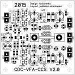
Here comes CDC-VFA-CCS V2
Preserving all the benefits of the 1-st version, here goes a refined version. Even less distortion, even more speed and versatility.
I will test this one myself - PCBs are coming tomorrow. Layout is half-SMD - all the active devices are TH, electrolytics are either SMD or TH.
Jeff, I took one of your layouts as a basis - helped a lot! Your overall parts placement is excellent.
This one can be easily used with wide range of OPS modules. I have simulated 3 options - for BJTs (EF3), IRFPs (with one EF) and Lateral FETs (direct drive) as the output devices. Slightly different VAS currents and compensation values are recommended.
This is almost a CFA-fast VFA
Test results and measurements will follow soon.
Cheers,
Valery
Preserving all the benefits of the 1-st version, here goes a refined version. Even less distortion, even more speed and versatility.
I will test this one myself - PCBs are coming tomorrow. Layout is half-SMD - all the active devices are TH, electrolytics are either SMD or TH.
Jeff, I took one of your layouts as a basis - helped a lot!
Your overall parts placement is excellent.This one can be easily used with wide range of OPS modules. I have simulated 3 options - for BJTs (EF3), IRFPs (with one EF) and Lateral FETs (direct drive) as the output devices. Slightly different VAS currents and compensation values are recommended.
This is almost a CFA-fast VFA
Test results and measurements will follow soon.
Cheers,
Valery
Attachments
VERTICAL front-end - back to the future!
And then I thought... why don't I try this great complementary (vertical) differential topology in a symmetric CFA front-end. I took my earlier CF-FET schematic as a basis and - voila!
Here comes the VERTICAL.
Key benefits:
1) Very high open loop linearity. No GNFB THD = 0.07% @ 20KHz, 20V RMS output (around 50W @ 8 Ohm). With the loop closed, the tallest harmonics (2, then 3) are close to -100db. Well - these are simulated values, but comparing to the other simulations - built ones - this is very good.
2) Rather high slew rate. Really difficult to say exactly at the moment, but it's high for sure. I will measure it at the live prototype later on.
3) Scalability - easy to have the output swing of the scale you want. Key regimes are independent from the rails voltage, having the input stage always supplied with +/-15V, so wide range of good low-noise low-voltage transistors can be used. With +/-75V rails, it's easily swings for having 250-280W of high-quality power @ 8 Ohm.
4) Versatility - easy to adapt to the wide range of the output stages of different topologies with different output devices, etc.
5) Simplicity. Initial CF-FET had 6 active devices, this one has got 8 - which is also not that bad.
It requires DC servo (not shown on the schematic here).
Working on the layout... coming soon It will be the same 3"x3" inch size, as the previous ones in this series.
The front-end is marked by the red frame.
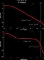
AC analysis is simulated for the whole amp - this time in combination with IRFP-based OPS.
Cheers,
Valery
And then I thought... why don't I try this great complementary (vertical) differential topology in a symmetric CFA front-end. I took my earlier CF-FET schematic as a basis and - voila!
Here comes the VERTICAL.
Key benefits:
1) Very high open loop linearity. No GNFB THD = 0.07% @ 20KHz, 20V RMS output (around 50W @ 8 Ohm). With the loop closed, the tallest harmonics (2, then 3) are close to -100db. Well - these are simulated values, but comparing to the other simulations - built ones - this is very good.
2) Rather high slew rate. Really difficult to say exactly at the moment, but it's high for sure. I will measure it at the live prototype later on.
3) Scalability - easy to have the output swing of the scale you want. Key regimes are independent from the rails voltage, having the input stage always supplied with +/-15V, so wide range of good low-noise low-voltage transistors can be used. With +/-75V rails, it's easily swings for having 250-280W of high-quality power @ 8 Ohm.
4) Versatility - easy to adapt to the wide range of the output stages of different topologies with different output devices, etc.
5) Simplicity. Initial CF-FET had 6 active devices, this one has got 8 - which is also not that bad.
It requires DC servo (not shown on the schematic here).
Working on the layout... coming soon
It will be the same 3"x3" inch size, as the previous ones in this series.The front-end is marked by the red frame.
AC analysis is simulated for the whole amp - this time in combination with IRFP-based OPS.
Cheers,
Valery
Attachments
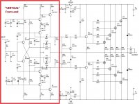
This one looks interesting. Is this output schematic going to become a board design soon too?And then I thought... why don't I try this great complementary (vertical) differential topology in a symmetric CFA front-end. I took my earlier CF-FET schematic as a basis and - voila!
Here comes the VERTICAL.
Key benefits:
1) Very high open loop linearity. No GNFB THD = 0.07% @ 20KHz, 20V RMS output (around 50W @ 8 Ohm). With the loop closed, the tallest harmonics (2, then 3) are close to -100db. Well - these are simulated values, but comparing to the other simulations - built ones - this is very good.
2) Rather high slew rate. Really difficult to say exactly at the moment, but it's high for sure. I will measure it at the live prototype later on.
3) Scalability - easy to have the output swing of the scale you want. Key regimes are independent from the rails voltage, having the input stage always supplied with +/-15V, so wide range of good low-noise low-voltage transistors can be used. With +/-75V rails, it's easily swings for having 250-280W of high-quality power @ 8 Ohm.
4) Versatility - easy to adapt to the wide range of the output stages of different topologies with different output devices, etc.
5) Simplicity. Initial CF-FET had 6 active devices, this one has got 8 - which is also not that bad.
It requires DC servo (not shown on the schematic here).
Working on the layout... coming soon
The front-end is marked by the red frame.
AC analysis is simulated for the whole amp - this time in combination with IRFP-based OPS.
Cheers,
Valery
This one looks interesting. Is this output schematic going to become a board design soon too?
Yes, I plan to make a layout for it as well - rather cheap and simple, but well-performing one
If you have time can you do a single sided too? I would like to try this but don't want another pile of PCB's to add to my collection. I don't mind some SMD pads. I can always add those on the bottom.
Thanks, Terry
Hi Terry, ok - I will try to make a single sided one, using some jumper wires...
Cheers,
Valery
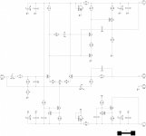
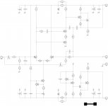
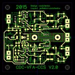
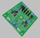
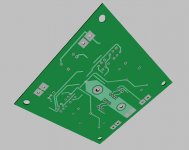
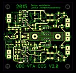
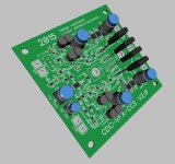
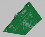
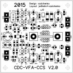
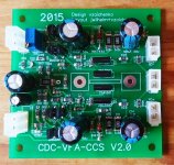
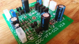
CDC-VFA-CCS V2.0 - built and tested standalone
Hello All,
My lab is roughly 30% back to life, so I have assembled and tested the latest version of CDC-VFA-CCS front-end.
Here is the schematic and PCB images "as built".
This one has got jFETs at the input. It's possible to use some low-noise BJTs as well - I will test that option later on.
Next post will present the measurement results.
Cheers,
Valery
Attachments

- Home
- Amplifiers
- Solid State
- Revisiting some "old" ideas from 1970's - IPS, OPS