Please forgive me if I am going about this incorrectly. I am new and this is my first post.
I recently purchased a Hafler Transnova 9300, this amp was stored for 15yrs due to the death of the previous owner. Internally it appears in excellent shape, it sounds great. I have searched the net and dont find much info.
I would really like the following:
owners manual PDF
Service manual pdf
Specs
Comments from anyone on any valid info on the amp
Copy of the magazine review on it, or how to go about obtaining it.
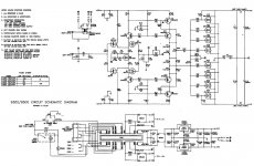
The Hafler brand name has been purchased by a new company, which for you means that all the old documentation is now available on line. Go to www.hafler.com, click on 'resources', then 'archive'. Scroll down and you will find all the old manuals in pdf form. There is no service manual per se, but the owners manual does include specifications, schematic, board layout and parts list. I wrote that manual and I insisted that such information be included!
The 9300 is a great amp rated at 150 wpc into 8 ohms, and is the little brother of the famed model 9500.
The 9300 is a great amp rated at 150 wpc into 8 ohms, and is the little brother of the famed model 9500.
One reason I bought a Hafler SE100 preamp is precisely because the users manual included a schematic and parts list. That Hafler made a general practice of this for most of their products only improved my high opinion of the company.
I think I'm reading a good bit of cascoding in this schematic. Not quite sure about the voltage amplifier stage, tho. A very straightforward design that's not any more complex than it needs to be; it ought to sound good.
Too bad you can't hardly find complementary JFETs any more.
I think I'm reading a good bit of cascoding in this schematic. Not quite sure about the voltage amplifier stage, tho. A very straightforward design that's not any more complex than it needs to be; it ought to sound good.
Too bad you can't hardly find complementary JFETs any more.
Did everyone spot how it gets 150w from 24v rail voltage ?
The output stage is fed from a higher voltage and does not behave as a voltage follower, the Mosfet sources being connected to ground. It has voltage gain and the output comes from the drains through the floating power supply, one for each channel. I discovered this scheme in the first Acoustat amp. Due to a negative/positive feedback, it had a very low output impedance.
The output stage is fed from a higher voltage and does not behave as a voltage follower, the Mosfet sources being connected to ground. It has voltage gain and the output comes from the drains through the floating power supply, one for each channel. I discovered this scheme in the first Acoustat amp. Due to a negative/positive feedback, it had a very low output impedance.
Indeed, the Hafler Transnova Series was designed by James Strickland, and was a direct descendent of his Acoustat TNT-200 and TNT-120 amplifiers. Transnova is an acronym for TRANSconductance NOdal Voltage Amplifier.
Troubleshooting Hafler Transnova 9300
I guess I will joint this thread rather than start a new one--but I hope the right people see my post.
I’m looking for help troubleshooting a Hafler 9300 I recently acquired.
Prior to hooking it up to anything I measured, among other things, the DC offset on the output. One side (left side) was very good at ~10 mV. The right side however had a huge offset of ~13 VDC. I am a relative newbie at circuit analysis so feel free to correct my understanding, but here’s what I’ve been able to figure out so far (and see attached schematic with measured values):

If Q1/Q2 and Q3/Q4 do need to be replaced, does anyone know a good substitute for 2SK163 and 2SJ74? Some of the recommended substitutes I’ve found so far are themselves unavailable.
I’ve heard that this amp can sound very good, so I’d like to get it working if possible?
Thanks for any help that can be offered.
Ron
I guess I will joint this thread rather than start a new one--but I hope the right people see my post.
I’m looking for help troubleshooting a Hafler 9300 I recently acquired.
Prior to hooking it up to anything I measured, among other things, the DC offset on the output. One side (left side) was very good at ~10 mV. The right side however had a huge offset of ~13 VDC. I am a relative newbie at circuit analysis so feel free to correct my understanding, but here’s what I’ve been able to figure out so far (and see attached schematic with measured values):
- The power supply seems to be in order with respect to voltages measured, with the exception that on the right side the large offset causes the nominal +/- 75 VDC to measure +87 and -60. So the rectifier output is close to correct, but the voltages referenced to ground are of by the offset amount.
- Taking some voltage reading with the amp on I find that the voltage on the gates of the input FETs are 0 on the Left side (the good side), but are quite high on the Right side. I.e the gate voltages on Q1 and Q3 are ~5VDC on the side with the large offset.
- I assume the large gate voltages on the input FET’s are the cause of the large offset on the output, and not the other way around. I know in some cases a bad cap on the feedback circuit can cause a DC offset on the output, but I don’t see how this could cause a voltage increase on the gates of the input FETs.
- Q1 or Q3 must be leaking in order to account for the voltage on their gates—is this a reasonable conclusion?
- If find these components difficult to measure while still in-circuit, but I could not find any obvious problems when measuring across different leads the transistors—i.e. no shorts or opens were detected.
If Q1/Q2 and Q3/Q4 do need to be replaced, does anyone know a good substitute for 2SK163 and 2SJ74? Some of the recommended substitutes I’ve found so far are themselves unavailable.
I’ve heard that this amp can sound very good, so I’d like to get it working if possible?
Thanks for any help that can be offered.
Ron
Attachments
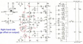
Check voltage on Q6 base (should be ~ +12v) and measure drop over R5 and R6 and calculate current.
Are there large offset on output?
Figge
Please check R8 is open circuit or not, and please measure voltages V1 and V2
It is possible R8 broken or a bad Q3 2SJ74
Thank you very much for your response.
Unfortunately I accidentally broke diode CR205. I ordered a new one but I cannot do any more measurement until it arrives.
I was able to measure r8 and it measured exactly in spec.
I will report back in a few days once my replacement diode arrives and I am able to make the measurements you suggest. Thanks again!
Ron
Diode is replaced so I'm back in business for troubleshooting.
Current over R5 and R6 is ~32mV based on dV of 1.51 and 1.52 respectively.
"V2" measures 18.21, which gives dV of 5.23, and I = 5mV.
Base of Q7 = -11.92, Emitter=-11.49, Collector=-23.83. So seems not enough bias to move any current--is that right?
R19 is measuring 750 instead of 1k (in circuit).
Thoughts?
Thanks!
Ron
Q6 base voltage is ~19.4 V (a bit high I guess).Check voltage on Q6 base (should be ~ +12v) and measure drop over R5 and R6 and calculate current.
Are there large offset on output?
Figge
Current over R5 and R6 is ~32mV based on dV of 1.51 and 1.52 respectively.
There is no dV across R10, yet it measures good resistance (1k)--so there is no current flow here!Please check R8 is open circuit or not, and please measure voltages V1 and V2
It is possible R8 broken or a bad Q3 2SJ74
"V2" measures 18.21, which gives dV of 5.23, and I = 5mV.
Base of Q7 = -11.92, Emitter=-11.49, Collector=-23.83. So seems not enough bias to move any current--is that right?
R19 is measuring 750 instead of 1k (in circuit).
Thoughts?
Thanks!
Ron
Base of Q7 = -11.92, Emitter=-11.49, Collector=-23.83. So seems not enough bias to move any current--is that right?
R19 is measuring 750 instead of 1k (in circuit).
Q7 and related resistors is normal, look like Q8 B/E shorted to give Q7 collector -23.83v
pls check Q8, if it shorted in B/E
Last edited:
Hi
if the input stage is working properly, the voltage at the input itself should be zero, but you have 5V there. Maybe the input gate leak resistor is open? It's the first thing to check after output offset.
In the original transnova amps, they used "anisotrpoic" feedback, which was supposedly a mix from two points but joined in a delta. I can't find the paper about it, but the only other signal point in the amp other than the speaker output is the gate drive node, which is opposite phase the output. Anisotropic means something like "different in opposite directions".
I'm not surprised Hafler would include schematics in the owner's manual since he was behind Dynaco when they were active.
- Status
- This old topic is closed. If you want to reopen this topic, contact a moderator using the "Report Post" button.
- Home
- Amplifiers
- Solid State
- Hafler Transnova 9300