Like the idea of the Cherry recommendation of running the power rails down the middle of the PCB. That way you can avoid all the sensitive electronics being inbetween the main sources of interference.
That's the kind of stuff I meant, most people just blindly place the rails to match the schematic. NOT optimal
Have to take a closer look. Don't have too much GM to play with...
The extra zeros from the capacitors do interact with the other compensation.
I don't yet have an analytical solution for the optimum, so it's iterative.
I would try to reduce the shunt stuff across the input.
There is no shunt in my own test-bed amp.
I first optimize the main feedback loop zero (from the capacitor).
Then tweak the LTP and Current mirror capacitors to try for whatever improvement I can.
But then re-experiment with the main loop.
Best wishes
David
That's the kind of stuff I meant, most people just blindly place the rails to match the schematic. NOT optimal
This was one my early learnings about loop areas etc... AndrewT suggested the Cherry method. It is deceptively easy to layout PCBs this way.
The extra zeros from the capacitors do interact with the other compensation.
I don't yet have an analytical solution for the optimum, so it's iterative.
I would try to reduce the shunt stuff across the input.
There is no shunt in my own test-bed amp.
I first optimize the main feedback loop zero (from the capacitor).
Then tweak the LTP and Current mirror capacitors to try for whatever improvement I can.
But then re-experiment with the main loop.
Best wishes
David
Sounds like a plan. Although in this amp it appears to be the shunts on the VAS output that dominate and the main loop compensation seems more like a fine tuning tweak. Maybe I should start again using your methodology and see where I end up.
When you say reduce the shunt stuff across the input do you mean C1 and R1?
I have simulated this and it did not work as well as I expected.
Those expectations were not just hope but based on simple theory, apparently TOO simple.
The unexpected bit was a result of source resistance, not revealed if one just tries an OPS driven from an ideal source.
Yes, I added a few comments about this after I pushed "submit" so we cross posted.
I try to put the posts up quickly but went a bit early.
So my failed attempts at using a CFP may not all be due to my limitations...
With this design as there isn't any current gain in the VAS a 3EF or similar is almost mandatory. Trouble is each stage adds it's own pole. Thought the CFP maybe a possible solution.
I noticed the cross post too... We both try and post quickly but 99% of the time I end up editing about 5 mins later when I realise I have made an error.
")
Paul
P.S. I like iterative processes. Can get a feel for how each part affects another.
... in this amp it appears to be the shunts on the VAS output that dominate... Maybe I should start ... and see where I end up.
A classic problem of optimization is to become stuck in a local optimum.
Kind of like when you want to reach the top of a mountain but if all you ever do is head upwards then you can end up on the top of a foothill.
A proper analytic solution would avoid this problem but I don't have it fully yet.
Thus I am somewhat reassured to see that your LTP and CM capacitors are similar values.
I usually end up with that too and it's unlikely we both found the same false optimum (I am not sure exactly why they are similar).
I essentially start with no compensation and look at the open loop, then proceed from there.
I think this avoids local minimums but it is still a bit too iterative/trial and error to really satisfy me.
When you say reduce the shunt stuff across the input do you mean C1 and R1?
Yes, but I would try to reduce any shunt compensation, why waste gain?
But sometimes one just has to burn some off, the AD797 seems to work OK
Here it may be the shunts on the VAS that you mentioned.
This is an effect of classic Two Pole compensation that is often not considered.
I think it explains why sometimes TPC is hard to beat.
Best wishes
David
Last edited:
A classic problem of optimization is to become stuck in a local optimum.
Kind of like when you want to reach the top of a mountain but if all you ever do is head upwards then you can end up on the top of a foothill.
A proper analytic solution would avoid this problem but I don't have it fully yet.
Thus I am somewhat reassured to see that your LTP and CM capacitors are similar values.
I usually end up with that too and it's unlikely we both found the same false optimum (I am not sure exactly why they are similar).
A proper analytical solution would be best but the maths would be a nightmare. Go back to Bode's book?
I know what you mean by getting stuck at a local optimum. It's a bit like refusing to re-evaluate a design by being too stubborn.
It is interesting that we ended up with similar values. Did notice that if you go too far with these capacitors you get a very dodgy looking LG plot.
I essentially start with no compensation and look at the open loop, then proceed from there.
I think this avoids local minimums but it is still a bit too iterative/trial and error to really satisfy me.
Yes, but I would try to reduce any shunt compensation, why waste gain?
But sometimes one just has to burn some off, the AD797 seems to work OK
Here it may be the shunts on the VAS that you mentioned.
This is an effect of classic Two Pole compensation that is often not considered.
I think it explains why sometimes TPC is hard to beat.
Best wishes
David
This amp is VERY sensitive to changes in C1 and R1.
When I look at TPC I see a shunt to GND is this a valid way of looking at TPC?
I think we are close to the limit though with this compensation unless some transistors are changed. The LG plot shows a pole at about 20KHz this appears to be a limitation. Most likely the output transistors? Changing the shunt compensation does not improve this.
So I shall try again using your methodology. I believe there is still more to be had from this design.
Paul
Optimisation - 2nd Attempt
Hi David,
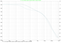
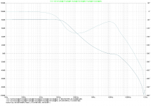
Have started the re-optimisation of this amp. The first stage has been to try and improve the open loop gain. All compensation has been removed. Here are two loop gain plots. One (hopefully) is the open loop gain and the other shows the effect of the capacitor across the feedback resistor. It does not look like this capacitor is the dominant part of the compensation.
Looks like the shunt compensation is the dominant part of the compensation for this amplifier.
Is my logic correct?
Paul
Hi David,
Have started the re-optimisation of this amp. The first stage has been to try and improve the open loop gain. All compensation has been removed. Here are two loop gain plots. One (hopefully) is the open loop gain and the other shows the effect of the capacitor across the feedback resistor. It does not look like this capacitor is the dominant part of the compensation.
Looks like the shunt compensation is the dominant part of the compensation for this amplifier.
Is my logic correct?
Paul
Attachments

Last edited:
...But is this bootstrapped shunt compensation on the VAS output actually a form of feed forward?
I don't think it is of importance here but you can check.
You can place the balun connections to see if there is any relevant feed-forward.
This would be in series with R39 and R40.
I have tried this on other amps and sometimes been surprised.
Classic Hawksford Error Correction does have major feed-forward.
As far as I can tell the classic analysis is seriously inaccurate because this is not considered.
But the results of feed-forward tests are sometimes not clear to me, which is a problem because it is the next level towards a more advanced model.
Bode (of course) does discuss this and it is precisely the point of Middlebrook's GFT probe.
Basically Bode and Middlebrook express the same conclusion, that once you have included feed-forward effects then you have a complete linear model.
So there is some consolation that it's not an endless task of ever more subtle effects to consider.
Best wishes
David
I think you are correct that the dominant factor in your simulated compensation is the bootstrapped VAS shunt.
Kind of TMC shunt.
Last edited:
I don't think it is of importance here but you can check.
You can place the balun connections to see if there is any relevant feed-forward.
This would be in series with R39 and R40.
I have tried this on other amps and sometimes been surprised.
Hi David,
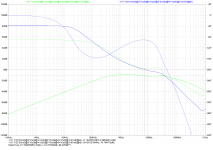
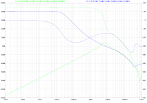
In the interests of science I have tried this on last night's re-optmisation. It looks strange as a compensation system but sims almost too well.
ULGF = 7.1 MHz
PM = 89 degrees
GM = 10.8 dB
See loop gain plot...
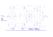
Also note the apparently incorrect by normal theory shunt capacitor values... 330pF bootstrapped by 680R from Predriver...??? Off a cascode VAS???
Is it worth a risk in reality?
But the results of feed-forward tests are sometimes not clear to me, which is a problem because it is the next level towards a more advanced model.
Bode (of course) does discuss this and it is precisely the point of Middlebrook's GFT probe.
I stand no chance then.
Basically Bode and Middlebrook express the same conclusion, that once you have included feed-forward effects then you have a complete linear model.
So there is some consolation that it's not an endless task of ever more subtle effects to consider.
Best wishes
David
And again we come round to the GFT Probe...
Suppose it's ineviteable when we both have a common interest in the control loops of amplifiers.
I think you are correct that the dominant factor in your simulated compensation is the bootstrapped VAS shunt.
Kind of TMC shunt.
Think it is really just a specialised two pole shunt. I'm thinking this isn't feedforward but just shaping the shunt response to compensate the amplifier (hopefully) effectively.
Have attached the usual various items for your (and others) perusal.
KR,
Paul
P.S. This amp is now taking nearly all my free time... Thread title massively inaccurate now.
Attachments
Last edited:
Paul, David - sorry for a "side" question - however, it is somewhat related to the point.
What do you think about the phase response curve "recession" - in this case at around 100-200KHz, pretty significant one (just some 22 degrees above 180 degrees phase "inversion")? In my designs I'm trying to arrange compensation in a way that it keeps the curve rather horizontal before it finally falls to 180 degrees crossing (at 35MHz in this case).
What do you think?
Thank you,
Valery
P.S. Edmond - I was typing at the same time with you So - question to you as well
What do you think about the phase response curve "recession" - in this case at around 100-200KHz, pretty significant one (just some 22 degrees above 180 degrees phase "inversion")? In my designs I'm trying to arrange compensation in a way that it keeps the curve rather horizontal before it finally falls to 180 degrees crossing (at 35MHz in this case).
What do you think?
Thank you,
Valery
P.S. Edmond - I was typing at the same time with you
So - question to you as well >Think it is really just a specialised two pole shunt. I'm thinking this isn't feedforward but just >shaping the shunt response to compensate the amplifier (hopefully) effectively.

Thought you'd come have a look at what was happening with your SuperTis front end?
Paul
Paul, David - sorry for a "side" question - however, it is somewhat related to the point.
What do you think about the phase response curve "recession" - in this case at around 100-200KHz, pretty significant one (just some 22 degrees above 180 degrees phase "inversion")? In my designs I'm trying to arrange compensation in a way that it keeps the curve rather horizontal before it finally falls to 180 degrees crossing (at 35MHz in this case).
What do you think?
Thank you,
Valery
P.S. Edmond - I was typing at the same time with you
This is typical for two pole compensation.
Paul, David - sorry for a "side" question - however, it is somewhat related to the point.
What do you think about the phase response curve "recession" - in this case at around 100-200KHz, pretty significant one (just some 22 degrees above 180 degrees phase "inversion")? In my designs I'm trying to arrange compensation in a way that it keeps the curve rather horizontal before it finally falls to 180 degrees crossing (at 35MHz in this case).
What do you think?
Thank you,
Valery
P.S. Edmond - I was typing at the same time with you
Hi Valery,
Side questions are fine in this thread.
Thank you for taking interest.
My personal thoughts on your question. Please bear in mind I'm still only a relative beginner in amplifier design.
This phase dip is caused by two pole compensation and the depth of the dip depends on how aggresively you use the two pole compensation.
22 degrees is quite tame for me. I find 10 degrees is enough. Even when transfered to prototype.
Sounds, to me, like you are desiging using single pole compensation. Or very tame two pole compensation?
Paul
Last edited:
Thank you guys for clarification.
Paul - I use two-pole in some designs. In one of them - phase margin is around 78 degrees, dip goes down to 45 - I have left it as is. In the other one (CFA) - I have tamed it almost completely up close to the margin level.
So, I was curios, if it's really worth taming it... looks like - I can relax
Thanks again,
Valery
P.S. Cool OPS arrangement
...What do you think about the phase response curve "recession" ...
... dip goes down to 45 - I have left it as is. In the other one (CFA) - I have tamed it almost completely up close to ...
As Damir, Paul and Edmond have already written, this phase dip is inherent to Two Pole.
It is not just unavoidable but actually part of the process.
There is a conservation law for total Phase (when expressed in the correct way with the Gain)
So if we want more PM at the Unity Gain Frequency then it must come from somewhere.
So we push down the phase far away to have more to "spend" where it matters.
If you "tamed" this phase dip then you defeat the entire point of two pole compensation.
And the only way to reduce the phase dip is to eliminate the second pole.
So it turns back into ordinary, dominant pole compensation anyway.
The trick is to know how to distribute the phase.
A phase of -180 (or even more*) is quite OK far from the ULGF but more of a problem as it becomes closer.
This is not so clear on a Bode Plot but easier to see on a Nichols Plot because Nichols has lines for equal Phase/Gain trade-off.
I think LTSpice can be made to show Nichols Plot but I haven't done it yet.
Maybe your simulator can?
Best wishes
David
* If the phase in the dip exceeds -180 then there is "conditional stability" in the strict, Nyquist sense of the term.
This sounds bad but can be perfectly acceptable.
It is not really necessary for an Audio amp so I prefer to avoid it.
I do, however, try to have the phase drop down fast as the frequency increases.
This depends on the Q of the two poles.
There is little analysis of this except by Dennis Feucht and his work is not quite accurate, omits effect of output load.
Any help appreciated!
Last edited:
Valery, you can relax. If you let the dip go below 0 degrees then you are then in the realms of conditional stability though.
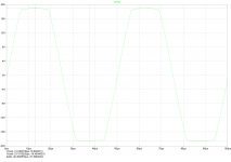
That OPS stage just happened. One thing concerns me is high frequency feed back through the collectors of the pre drivers. Do think a high frequency filter would be worth having. The price being paid is performance though. What do think?
One last bit of fun for today... The MIC version. Can it be done without a proper PCB?
Here it is...
ULGF = 7.5MHz
PM = 106 degrees (I think-plot attached anyway)
GM = 15 dB
Paul
That OPS stage just happened. One thing concerns me is high frequency feed back through the collectors of the pre drivers. Do think a high frequency filter would be worth having. The price being paid is performance though. What do think?
One last bit of fun for today... The MIC version. Can it be done without a proper PCB?
Here it is...
ULGF = 7.5MHz
PM = 106 degrees (I think-plot attached anyway
)GM = 15 dB
Paul
Attachments
So if we want more PM at the Unity Gain Frequency then it must come from somewhere.
Now it's perfectly clear, all the parts of the "picture" came together and took their places - many thanks.
Maybe your simulator can?
I will see if Multisim has got something "built-in" for this.
David,
Could the "MIC" loop be feed forward? It has a gain greater than one at the frequencies that matter.
Hope the V(z0) probe is in the right place?
As you can see I stripped out the front end... Didn't see the need, already had plenty of PM.
Paul
Could the "MIC" loop be feed forward? It has a gain greater than one at the frequencies that matter.
Hope the V(z0) probe is in the right place?
As you can see I stripped out the front end... Didn't see the need, already had plenty of PM.
Paul
Attachments
Now it's perfectly clear...many thanks
A pleasure.
Could the "MIC" loop be feed forward? It has a gain greater than one at the frequencies that matter.
You do like circuits with multi-way feedback connections (to the VAS, to the Input and to the OPS) that really make me think
But am relaxed about this one because the response in this loop is "textbook".
In particular, the phase looks pleasantly understandable, just simple minimum phase.
We know that feed-forward can potentially produce RHP zeroes, in other words "excess phase", in the strict use of the term.
So if there is no evidence of excess phase then I assume the feed-forward is so small that a simple analysis is fine and the complication of a Middlebrook GFT analysis is not needed.
On your post #48 you showed the shunt VAS loop to look for feed-forward there.
I think there is just a trace of non-minimum phase there, based only on visual estimate.
A second "To Do" is to work out how to plot excess phase in LTSpice.
In this case not critical because the loop gain is always small.
Hope the V(z0) probe is in the right place?
We learn about some loop no matter where you put it.
As you can see I stripped out the front end... Didn't see the need, already had plenty of PM.
Yeah! My own development example has MIC and no front-end shunt.
So my recommendations naturally tend to lead in that direction.
But I hope you will find that it does perform better on objective metrics.
That would confirm that it's simply a better idea and not just my prejudices that have mislead you.
Best wishes
David
Last edited:
- Status
- This old topic is closed. If you want to reopen this topic, contact a moderator using the "Report Post" button.
- Home
- Amplifiers
- Solid State
- Amp designed during lunch breaks