Hello All,
"As built" version is >HERE<
Following is my initial post:
_____________________________________
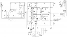
Based on successful prototyping of the first hybrid with tube-based LTP input stage, I'm moving forward, trying to utilize the advantages of "both worlds". Tube-based front-end, performing all the voltage gain, and solid-state power section (class A unity voltage gain buffer), designed by Damir (the best one I'm aware of), performing all the current gain. Trying to keep the whole thing as simple as possible.
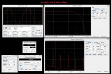
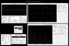
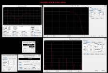
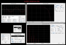
Here are some initial simulation results. Look very promising.
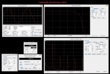
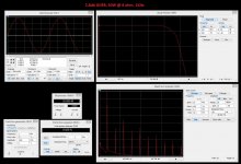
Voltage gain is set to standard 29db
OPS quiescent current is 2.2A
Attached pictures show the schematic and some simulations.
First option is purely NO GNFB - only some cathode degeneration. Tubes at their best.
Second option - same schematic with 2.8db gain increase at the second stage and then dropping the same amount with GNFB. Slightly reduced distortion, however - not too much difference, so... just as an experiment. Attempts to further increase the open loop gain and compensate it by GNFB result in overall distortion increase (12au7 is a relatively low gain tube, high linearity though).
I really like very low THD increase between 1KHz and 20KHz at all levels.
Any thoughts, comments, ideas will be greatly appreciated.
Cheers,
Valery
"As built" version is >HERE<
Following is my initial post:
_____________________________________
Based on successful prototyping of the first hybrid with tube-based LTP input stage, I'm moving forward, trying to utilize the advantages of "both worlds". Tube-based front-end, performing all the voltage gain, and solid-state power section (class A unity voltage gain buffer), designed by Damir (the best one I'm aware of), performing all the current gain. Trying to keep the whole thing as simple as possible.
Here are some initial simulation results. Look very promising.
Voltage gain is set to standard 29db
OPS quiescent current is 2.2A
Attached pictures show the schematic and some simulations.
First option is purely NO GNFB - only some cathode degeneration. Tubes at their best.
Second option - same schematic with 2.8db gain increase at the second stage and then dropping the same amount with GNFB. Slightly reduced distortion, however - not too much difference, so... just as an experiment. Attempts to further increase the open loop gain and compensate it by GNFB result in overall distortion increase (12au7 is a relatively low gain tube, high linearity though).
I really like very low THD increase between 1KHz and 20KHz at all levels.
Any thoughts, comments, ideas will be greatly appreciated.
Cheers,
Valery
Attachments
-
 @LinearGain-Hybrid-01-NoGNFB-00-sch.jpg218.8 KB · Views: 1,650
 -
 @LinearGain-Hybrid-02-GNFB-2.8db-50W-20k.JPG359.9 KB · Views: 182
 -
 @LinearGain-Hybrid-02-GNFB-2.8db-50W-01k.JPG371.3 KB · Views: 523
 -
 @LinearGain-Hybrid-02-GNFB-2.8db-00-sch.JPG241.9 KB · Views: 590
 -
 @LinearGain-Hybrid-01-NoGNFB-50W-20k.JPG379.9 KB · Views: 1,070
 -
 @LinearGain-Hybrid-01-NoGNFB-50W-01k.JPG371.2 KB · Views: 1,141
 -
 @LinearGain-Hybrid-01-NoGNFB-10W-20k.JPG372.6 KB · Views: 1,242
 -
 @LinearGain-Hybrid-01-NoGNFB-10W-01k.JPG364.2 KB · Views: 1,556
Last edited:
Member
Joined 2009
Paid Member
Hi,
I wondered about the RC-lowpass (100R/150p) at the Szikay´s Master transistor Bases (Q3,4).
I rather know the compensation as single cap or as RC from the Collector to the Base of the Slave transistor (Q5,6) or in parallel to the Master´s collector resistor (R14,17).
Is there an advantage using the bandwidth limiting RC at the Bases, instead of local (or internal) compensation?
What were the parameters for choosing the VD139/140 and MJL1302A/3281A?
They are rather slow and the MJLs not low capacitance devices.
This might lead to oscillation of the Sziklay pair at rather lowish frequencies)
R14/17 are fortunately very low in value, but still low-cap power transistors might be a good alternative, for example 2SA1186/SC2387 (Sanken, ISC).
The 2SB649/2SD669 driver transistors can drive a pair of 1186/2837 each (R14,17=150R, added 0R22 Emitter resistors for 1186/2837 and R3,9=0R22)
jauu
Calvin
Last edited:
Hi Calvin,
As I mentioned in the first post, the output buffer is actually designed by Damir - I just slightly modified it, adding second output pair. 100R/150p are acrually a base stopper and shunt compensation capacitor, forming a roughly 10MHz low pass filter, as you mentioned, ensuring stability of Sziklai pairs. This choice of transistors was Damir's choice, however I have simulated the whole thing and it shows excellent performance, including the bandwidth and level of distortion. I also know that this buffer was built by Damir and some other people here with very good impressions.
I also like Sankens and use them frequently, however in this case I just use a successful design. My major interest in this project is to test the sound of tube-based voltage gain stage with no global NFB.
Cheers,
Valery
Hi Calvin,
As I mentioned in the first post, the output buffer is actually designed by Damir - I just slightly modified it, adding second output pair. 100R/150p are acrually a base stopper and shunt compensation capacitor, forming a roughly 10MHz low pass filter, as you mentioned, ensuring stability of Sziklai pairs. This choice of transistors was Damir's choice, however I have simulated the whole thing and it shows excellent performance, including the bandwidth and level of distortion. I also know that this buffer was built by Damir and some other people here with very good impressions.
I also like Sankens and use them frequently, however in this case I just use a successful design. My major interest in this project is to test the sound of tube-based voltage gain stage with no global NFB.
Cheers,
Valery
Valery, you can take a look at my last schematic in GainWire-CLASS-A power amp (I am out of my house and using tablet to sent this answer and dont know how to copy the link with it) and see that I used the diamond instead Baxandall super pair as Elwee suggested, more stable with CFP.
Valery, you can take a look at my last schematic in GainWire-CLASS-A power amp (I am out of my house and using tablet to sent this answer and dont know how to copy the link with it) and see that I used the diamond instead Baxandall super pair as Elwee suggested, more stable with CFP.
Hi Damir!
Do you mean the one with diamond and bootstrap from the post #60 there?
Thank you,
Valery
Hi Damir!
Do you mean the one with diamond and bootstrap from the post #60 there?
Thank you,
Valery
Hi Valery, Yes it is the post #60, but you dont need to use bootstrap, try to simulate with the square wave.
Damit
Hi Valery, Yes it is the post #60, but you dont need to use bootstrap, try to simulate with the square wave.
Damit
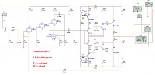
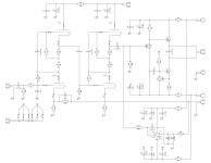
Damir, you're right - this way it shows better stability. I have also decreased the base stoppers value to 10 ohms and shunt caps to 47pF, as you suggest in the latest schematic, and it actually stays stable even without the caps, being close to margin though. With 47pF caps in place it looks excellent.
Also changed the CCS output transistors to 2N5401/5551 as with my +/-36V rails BC550/560 run out of SOA in case of high output swing.
Started preparing for prototyping. I will build the front-end and the buffer at separate PCBs, so that I can experiment with different combinations. This is going to be interesting
")
Cheers,
Valery
Attachments
Hi,
I wondered about the RC-lowpass (100R/150p) at the Szikay´s Master transistor Bases (Q3,4).
I rather know the compensation as single cap or as RC from the Collector to the Base of the Slave transistor (Q5,6) or in parallel to the Master´s collector resistor (R14,17).
Is there an advantage using the bandwidth limiting RC at the Bases, instead of local (or internal) compensation?
What were the parameters for choosing the VD139/140 and MJL1302A/3281A?
They are rather slow and the MJLs not low capacitance devices.
This might lead to oscillation of the Sziklay pair at rather lowish frequencies)
R14/17 are fortunately very low in value, but still low-cap power transistors might be a good alternative, for example 2SA1186/SC2387 (Sanken, ISC).
The 2SB649/2SD669 driver transistors can drive a pair of 1186/2837 each (R14,17=150R, added 0R22 Emitter resistors for 1186/2837 and R3,9=0R22)
jauu
Calvin
Hi
Where do you found 1186 ?
I would like made a CFP power buffer

Hi,
distributor Reichelt has listed the Inchange Semi for 1€/pcs. and also the complementary 2SC2837.
The 2SD667/2SB647, smaller brethren of the D669/B649 with more linear hfe, are listed too for 25 €cent.
A CFP is a bit prone to oscillation and some transistor combinations require compensation.
It is good use to choose the power-slave a fast low-capacitance type and the collector resistor of the master-driver low ohmic, as we want the pair to be fast -at least when its part of a rather classical global-FB amplifier.
In a Non-gFB design the requirement for speed may be somewhat lower.
The combination of the B649 with two C2837, resp. D669 and two A1186 is used succcessfully in the L12-2 amp by LJM, one of the very few amplifier modules on the market, capable to drive even severe loads like my enigmatic Electrostats not only fully stable but also sonically well.
jauu
Calvin
ps. just seen the CF-triple Diamond Buffer.
Take care though, that thing will probabely oscillate.
A CFP will suffice here anyway, so don´t make it more complex than required
Last edited:
To get a full valve sound you need front end, phase splitter, class AB output stage and output transformer.
I have designed a couple of hybrids and they never sound like a pure valve amplifier.
Hi Nigel,
In fact, I don't have a goal to reach a pure valve amplifier sound.
I'm trying to utilize the benefits of "both worlds" - tubes are very good in voltage gain stages. As tubes are more linear than SS devices, and wide-bandwidth enough, it's possible to design a highly linear voltage gain stage with no global NFB. As a result, we get high stability and hopefully certain "tube flavor".
On the other hand, SS output stage provides high-currents capability, low output impedance, high power (if required) and (especially in class "A") high linearity. Output buffer I'm trying to use is expected to be as "transparent", neutral, as possible, providing linear current amplification (and close to unity voltage gain).
Looking forward to hearing what it sounds like
Cheers,
Valery
Coming closer to live prototype
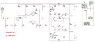
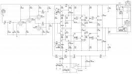
OK, after some more research, I have come to the following solution (see attached schematic). Voltage gain is purely tube-based, in two SRPP stages. Nested feedback with very light global loop, gains are as follows:
1-st stage OLG: 15.6 db
2-nd stage OLG: 22.2 db
Overall OLG: 37.8 db
Closed loop gain: 29.3 db
Global loop gain: 8.5 db (only!)
3-rd stage is a unity gain buffer for better coupling with OPS (making it virtually independent from the power section used). Also includes DC servo, sensing the power section output. Later on, it will be possible to test the front-end with different power sections, choosing the best combination.
All stages are single-ended, highly linear.
All compensation is just a single 2.2 pF lead capacitor, limiting the overall bandwidth at roughly 100 KHz and providing appropriate phase shift.
If I manage to get away with this in practice, that will be cool.
This is not the final version, mostly for discussion - will most likely be updated after prototyping.
Cheers,
Valery
P.S. Gareth, you'll like it, I believe
Attachments
Member
Joined 2009
Paid Member
It's coming along nicely !
Depending on the OPS design I'm interested to know why you need the unity gain buffer ?
That unity gain buffer is a great topology, the JLH69 is an amplifier I hope to finish and I have made my version of it with the option to flip it into a unity buffer just like the one you have !
Why not make it all Class A, forget the OPS and just beef up that buffer - it would be a nice amplifier already.
It's coming along nicely !
Depending on the OPS design I'm interested to know why you need the unity gain buffer ?
That unity gain buffer is a great topology, the JLH69 is an amplifier I hope to finish and I have made my version of it with the option to flip it into a unity buffer just like the one you have !
Why not make it all Class A, forget the OPS and just beef up that buffer - it would be a nice amplifier already.
This is also an option - probably will require one more current-gain stage, working from 2A CCS or close to it. Actually, it's a pretty "universal" thing - you can use it and enhance it, the way you like, or you can just skip it, if your external OPS is rather high-impedance...
Member
Joined 2009
Paid Member
I found this interesting
JLH Class A revealings - Audio Forum | Graham Slee Online Owners Club - Page 1
seems the JLH output is a 7400 TTL !
JLH Class A revealings - Audio Forum | Graham Slee Online Owners Club - Page 1
seems the JLH output is a 7400 TTL !
- Status
- This old topic is closed. If you want to reopen this topic, contact a moderator using the "Report Post" button.
- Home
- Amplifiers
- Solid State
- lGl-2, continuing "hybrid madness" - no GNFB class A