R465 - R468 (68 ohm) open circuit
Dear all,
Many thanks for all the tips, experience and troubleshooting advice on the NAD3240PE.
In August 2020, I started with L power amplifier channel no output. The pre-amp section was tested fine. After recapping all the electrolytic caps and signal path caps, still no good. Power supply voltages were good, and I checked no fuses were blown.
Then on a power on circuit test, I accidentally touched my meter probe a power trace on the printed board and blew the R (good) channel transistors Q418, Q420, Q422, Q424 & Q426.... sigh, I then put the project aside since last October.
Then in early April this year, I found out that R465 - R468 were open circuit (!)... after searching, I managed to get new output power transistors for both L & R channels from various sources in eBay. Replaced all then did the alignment and idle current checks per the service manual; both channels are good now. Will try to test with signal next...
It was almost a full circle of effort, I could have checked those resistors first before doing a tedious recap.
Just a newbie that is trying to bring the almost 20 years old NAD to life again.
Johan 64 - post #60
Hi Johan 64,
From the 3240PE circuit schematic, with bass, treble knobs at neutral (ie. 12 o’clock); mono button out, balance at neutral, tape monitor not pressed and Bass EQ not pressed - the functions you mentioned is effectively bypassed, as the inputs from the volume control go straight through the NJM2043 pre-amp chip and then out to the JFETs (output of the pre-amp).
Appreciate if the rest can confirm? Thanks all!
Right channel nil sound output
Dear all,
Appreciate your advice.
The right channel goes off again (no sound produced).
I replaced all the transistors in the input section of the power amp (2SA970s & 2SC2240s), bridge rectifier and tested power supply caps C505/C506 ok.
The Centre adjustment using VR402 started with 40V, and I couldn’t adjust it down to 0 +/- 30 mV. The lowest was 13V. The voltage at the right channel speaker terminals seems to get lower at first, then goes up and stagnates then goes up again.
At the last connection to speakers before troubleshooting, loud pops could be heard when switching from speakers A to B and vice versa. I disconnected the speakers since, to prevent damage. Strangely, this loud pops occurred when I retouched them solder connections on the right channel. I measured all transistors in-situ and don’t seem to find any shorted junctions. All diodes also seem ok with 0.7 V drops. Previously was only no sound from the right channel. Seems worse off after retouching the solders on the PCB.
The left channel has no issues. +3 mV adjusted since my earlier posts.
Appreciate if you guys could shed some light and advice the next steps in troubleshooting.
Thanks all.
R Channel root defect - break in PCB track
Dear all,
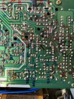
Defect in R channel high DC offset is due to a break in the PCB track, from the bases of Q412/Q416 to R442. I discovered it by chance when checking for continuity after replacing both transistors.
This was after futile attempts (changing zener diodes, BD501, all low power transistors - 2SA970s & 2SC2240s).
After bridging with a component lead (see photo, break is at the track indicated by a red arrow).
This brings a good closure to this, after more than a year!
Dear all,
Defect in R channel high DC offset is due to a break in the PCB track, from the bases of Q412/Q416 to R442. I discovered it by chance when checking for continuity after replacing both transistors.
This was after futile attempts (changing zener diodes, BD501, all low power transistors - 2SA970s & 2SC2240s).
After bridging with a component lead (see photo, break is at the track indicated by a red arrow).
This brings a good closure to this, after more than a year!
Attachments
Dear all,
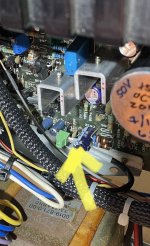
I managed to nail down the R channel intermittent issue to the PCB pre-amp to power amp connector, which I replaced (see photo with yellow arrow). The contact was having high resistance.
I ended replacing the L channel too. I’m confident I resolved all the R channel issues finally (I now know for sure!).
Happy New Year all!
Best regards,
Sim T.
Attachments
There are obviously different service manuals. For the mentioned error in the right channel please refer the first pdf attachment.There is an error in the clean version of the schematic. With regards to R466 the left channel (R465) is correct, the right channel is not.
The node A, D418/C424/C, Q420 is wrong (short C-B Q420).
C424/C, Q420 must be connected to the pos. 70V rail behind R466, i. e. to positive pole of elcap C430 (10/100)
In the schematic version of second pdf attachment there isn't to find this error drawing in the right channel.
Attachments
Now I have a device of this model on the desk with differences zu both service manuals from the pdf attachments in my previous post, which are in turn different (now I know three different versions - concerns only class G piggyback unit) :
part-No first PDF sec. PDF own device
==========================================
Q431/Q432 2SB826 2SB826 BD912
Q433/Q434 2SD1062 2SD1062 BD911
Q435/Q436 2SB649 2SB649 BD680 (Darlington)
Q437/Q438 2SD669 2SD669 BD679 (Darlington)
R489/R490 15K 15K 2K2
R491/R492 15K 15K 2K2
C437/C438 100p 100p 39p (390)
C439/C440 100p 100p 39p (390)
C433/C434 330p 150p 1200p (122)
C435/C436 330p 150p 1200p (122)
C441/C442 330p 100p 560p (561)
C443/C444 330p 100p 560p (561)
Are there service-bulletins, where the various upgrades mentioned (there are probably many more variations than those I have mentioned here) ?
P.S.: Unfortunately space bars (blank space) does not transfer so that what is written from me appears as a table.
Last edited:
- Home
- Amplifiers
- Solid State
- DIY includes repair? NAD 3240PE advice needed...