Cortez,
on you spice model, what the output looks like if you adjust rca and pcb-psu ground cable resistances so that the rca cable reistance is 10x of the pcb-psu? now its just 2x. And what it looks like if the ratio is 100x (eg. very short wire from per amp starground to ps ground)?
Can you add the hum reducing resistor between rca input ground wire and audio ground, how much effect it has?
What if there was a short between rca input grounds: if the rca inputs were next to each other in the amp chassis and connected with a wire?
How the poweramp ouput return current affects?
thanks
Last edited:

")
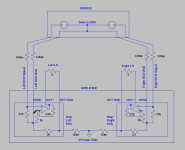
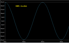
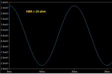
Yes, the 2 x 10R HBR works of course, as this version shows, my
original question was aimed to FirstWatt users where this isn't used.
I guess they don't tolerate any major hum in this category so I was curious
to the reason why there isn't hum despite to this trivial layout "error"...
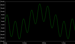
2nd image shows the current on the interconnect GND wire reduced to the mA range.
BTW: if anyone has such a layout (2 channels with common PSU using 10R hum
breaking resistor)
I'd be intrested for a real life measurement with a oscope on the 10R during music...
original question was aimed to FirstWatt users where this isn't used.
I guess they don't tolerate any major hum in this category so I was curious
to the reason why there isn't hum despite to this trivial layout "error"...
2nd image shows the current on the interconnect GND wire reduced to the mA range.
BTW: if anyone has such a layout (2 channels with common PSU using 10R hum
breaking resistor)
I'd be intrested for a real life measurement with a oscope on the 10R during music...
Attachments
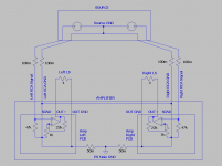
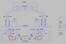
And this is the other version when there is no 10R HBR but
the 2 RCA GND is connected together inside the amplifier.
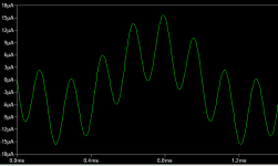
2nd image: interconnect GND current
3rd image: RCA GND shunt current
the 2 RCA GND is connected together inside the amplifier.
2nd image: interconnect GND current
3rd image: RCA GND shunt current
Attachments
Problem: how a layout like above can work without these resistors.
Look here for example.
There is a giant GND loop, the trafo is in the center, and I guess there is no hum at all.
Why...?
No one is saying there is no hum at all, just that it is made minimal.
If you want perfection in this regard, you go to mono blocks.
Two more points,
Actual resistance to ground in the F7 is 10 mohm not 50, which lowers
your numbers by a factor of 5.
Also, it might be useful for you to explore the actual differential output
of the amplifier model as opposed to ground currents. This would show
up in an ordinary cross-talk measurement.
Actual resistance to ground in the F7 is 10 mohm not 50, which lowers
your numbers by a factor of 5.
Also, it might be useful for you to explore the actual differential output
of the amplifier model as opposed to ground currents. This would show
up in an ordinary cross-talk measurement.
And what about the conventional 10R HBR (hum breaking resistor) solutionNo one is saying there is no hum at all, just that it is made minimal.
between the Signal and the Power GND points on the PCB?
Do you have any bad experiences regarding to sound quality?
I tried it with 10mohms and even in this case there is a groundTwo more points,
Actual resistance to ground in the F7 is 10 mohm not 50, which lowers
your numbers by a factor of 5.
current around 400mA flowing via the interconnect GND wires.
The 10R HBR resistors should decrease this even more.
Or another solution could be: connecting the RCA GNDs right at the amplifier
rear panel and tie it right to the PSU GND and then no Signal - Power GND connection
would be necessary on the Amplifier PCB. What's your opinion about this layouts?
Sorry, I didn't understand this point. What does "differential output" mean in this context?Also, it might be useful for you to explore the actual differential output
of the amplifier model as opposed to ground currents. This would show
up in an ordinary cross-talk measurement.
What should I explore?
Yeah, we know that, it's not clear: how should I interpret your post? What is the conclusion?
No conclusion. If you look at the voltage over the load you will see that the hum is present even without an input signal. Play with the configuration to see if you can reduce this output signal. Your simulations do not show ground loop but something entirely different.
Thanks Mark, I understand now.
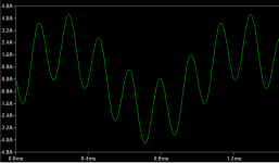
I played with your layout (the inductive coupling added) and here are the results
applying the 2 different resistor values (1u vs 10R) between the Signal and Power GND.
Although I'm not sure about the L1, L2, L3, K numbers in real life, are they correct?
I played with your layout (the inductive coupling added) and here are the results
applying the 2 different resistor values (1u vs 10R) between the Signal and Power GND.
Although I'm not sure about the L1, L2, L3, K numbers in real life, are they correct?
Attachments
I just copied/guessed the numbers. Even the 50 Hz current is not correct as it would be spikey because of charging the PSU capacitors. What about other sources of EM and do the interconnects not also pickup?
It is all going to depend on the layout and the transformer used. Did you see that Nelson uses a CL60 in series with the transformer primary? This is also going to change the current through the transformer.
For me, it is about getting a better understanding of how things work.
It is all going to depend on the layout and the transformer used. Did you see that Nelson uses a CL60 in series with the transformer primary? This is also going to change the current through the transformer.
For me, it is about getting a better understanding of how things work.
I link my summary post from the other topic just to have it here as well.
Yes, it's a great article and summary for this kind of issues....and the hifisonix paper you linked to earlier is very good...
My only concern which I'll investigate soon is about using the HBR is
regarding the "feedback current path" which is very critical as we all know.
1st issue can be: with high current feedback loops (aka CFAs or the FirstWatt designs)
as a significant voltage is generated on this resistor related to the main GND.
Even around 1 volt...
2nd issue: the feedback current path has also a loop created:
PS -> Amp PCB -> FB resistors -> Signal GND -> PS GND
If this loop is big enough (which it easily can be as we often try to
place the high current PS wires far from the sensitive input wires...)
then this loop will have a significant parasitic inductance which can affect HF performance.
I'll draw an image later about this effect.
Last edited:
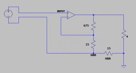
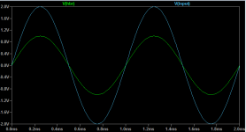
Here is the simulation for the 1st issue:
Using a 15R HBR resistor the input GND will be "lifted" according to the FB current.
On the 2nd image you can see the absolute voltages (related to GND) at the HBR
and the opamp input nodes. As you can see there is a common mode input signal as well.
I'm not sure how a CFA for example handles such kind of input signal.
Attachments
You might want to check out Tomchr's work LM3886 chip amp grounding. and LM3886 PCB vs Point-to-Point (with data) for more insight.
THD and Noise will depend on layout. Where to connect the speaker return is the next question.
THD and Noise will depend on layout. Where to connect the speaker return is the next question.
- Status
- This old topic is closed. If you want to reopen this topic, contact a moderator using the "Report Post" button.
- Home
- Amplifiers
- Solid State
- Multichannel amplifier internal ground loop