My 2 cents.
I would actually get rid of R8 and R17. Just connect the base of Q6 to emitter of Q5, collector of Q9 to the ground.
R7 depends on the CCS current you would like to have for the LT, let say you want 2mA (1mA per each side of the pair), then it will be roughly 600mV / 2mA = 300 Ohm (330 will be ok).
Now, I would calculate R18 and R19 values in reverse order.
I would choose R19 as 22R (it is also a local NFB for Q8 - 22 is a practical minimum based on experience, just for stability reasons).
Quiescent current for VAS is roughly 600mV / 100 Ohm (R12) = 6 mA.
In this case V at R19 will be 6mA * 22 Ohm = 132 mV.
V at R18 will be 132 mV + 600 mV = 732 mV.
Assume Q9 quiescent current 1mA, then R18 = 732 mV / 1 mA = 732 Ohm (ok, use 680 Ohm, will give you 732/680 = 1.08 mA).
One more point - overall gain and global NFB.
Standard gain for the power amp is 29 db, which is equal to roughly 28 (Vout/Vin).
Gain = R33 / R9 + 1, meaning you need to use R33 = 27k.
It will also most likely require additional compensation - some 10-15 pF cap in parallel with R33. You will determine the optimal amount looking at square wave output (smaller capacitor will result in "undershoot", bigger one - "overshoot").
In overall - a pretty working setup.
Good luck!
BR,
Valery
Last edited:
Keep R8 and R17.
You may need them.
If you do add a small NP0 in parallel to R33 then allow pads for a series connection of R+C.
The R helps eliminate oscillation.
Don't worry about actual values at the moment.
That can come much later.
It's locations for the components on the final PCB that are important now. You have to live with the final PCB for all your implementations that come later.
You can experiment with component values in a simulator to help you reach conclusions on (typical) values to be adopted in the first prototype.
I don't know what voltages you plan nor whether smd, or through hole, but allow for series connecting the feedback resistor. Try two in series as a first guess for power capability and minimising temperature changes with output levels and reducing the voltage across each resistor.
Last edited:
Andrew, I'm using a spare DX blame mkiii board for this project so topology and component locations are fixed. I can delete components with wire links but not add.
The purpose of this exercise is to come up with optimal R and C values for a so-called blameless design. I'd prefer not to use a simulator
56V rails per schematic.
The purpose of this exercise is to come up with optimal R and C values for a so-called blameless design. I'd prefer not to use a simulator
56V rails per schematic.
Last edited:
forr, I selected 47k for input and feedback resistors to present high input impedance and lowest RC corner frequency with 1uf film input cap. I can substitute 22uf bipolar and reduce R values accordingly if this is unacceptable.
R33 and r9 were calculated to give peak 150W output power with 1Vrms input.
R33 and r9 were calculated to give peak 150W output power with 1Vrms input.
Calling AndrewT...
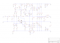
As built schematic attached. I'm running a single pair of output devices with 35VDC rails.
With the trimpot adjusted to give 26mV bias across each output emitter resistor:
Output offset is -78mV.
+ve driver emitter = 540mV
-ve driver emitter = -654mV
I believe there is a problem with my Vbe resistor values as the driver bases are unbalanced and increase/decrease as a function of the trimpot value.
+ve driver emitter = 0.83 * -ve driver emitter
Vdrop OP emitter = 11mV; +ve emitter = 507mV; -ve emitter = 620mV
Vdrop OP emitter = 26mV; +ve emitter = 540mV; -ve emitter = 654mV
Vdrop OP emitter = 51mV; +ve emitter = 540mV; -ve emitter = 654mV
Vdrop OP emitter = 109mV; +ve emitter = 633mV; -ve emitter = 748mV
Attachments
Last edited:
forr, I selected 47k for input and feedback resistors to present high input impedance and lowest RC corner frequency with 1uf film input cap. I can substitute 22uf bipolar and reduce R values accordingly if this is unacceptable.
R33 and r9 were calculated to give peak 150W output power with 1Vrms input.
I think that with the current resistor values, the performances are acceptable (however the output DC is rarely as high) but not optimal towards the general blameless philosophy.
R1 (currently 2.2 kOhm) should be of a value near to R9 (currently 1 kOhm).
For DC balanced, non-inverting input current flows through R1+R2 = 49.2 kOhm as inverting input current flows through R33 = 47 kOhm.
I would place R1 ahead of R2 at the expense of a loss (0.4 dB for 2.2 kOhm) of the input signal.
In his book about power amplification, Self shows an increase of distortion with an increase of source impedance (6th edition, page 144), more than 6 dB between 50 Ohm and 2.2 kOhm at 1 kHz.
For the needed voltage gain, 34.6 times, I would choose the following values :
R1 = 10 kOhm
R2 = 330 Ohm
R33 = 10 kOhm
R9 = 330 Ohm
C6 = 680 µF or more
C1 = 4.7, 10 µF or more (possibly bipolar)
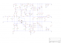
could you add some resistor Vdrops to your sch?
Vr5&6, Vr18, Vr19, Vr3&4, Vr7, Vr12, Vr16&20, Vr37
and Vc2, Vc6
Andrew, refer attached. Thanks in advance for any suggestions you can offer.
Attachments
I think that with the current resistor values, the performances are acceptable (however the output DC is rarely as high) but not optimal towards the general blameless philosophy.
R1 (currently 2.2 kOhm) should be of a value near to R9 (currently 1 kOhm).
For DC balanced, non-inverting input current flows through R1+R2 = 49.2 kOhm as inverting input current flows through R33 = 47 kOhm.
I would place R1 ahead of R2 at the expense of a loss (0.4 dB for 2.2 kOhm) of the input signal.
In his book about power amplification, Self shows an increase of distortion with an increase of source impedance (6th edition, page 144), more than 6 dB between 50 Ohm and 2.2 kOhm at 1 kHz.
For the needed voltage gain, 34.6 times, I would choose the following values :
R1 = 10 kOhm
R2 = 330 Ohm
R33 = 10 kOhm
R9 = 330 Ohm
C6 = 680 µF or more
C1 = 4.7, 10 µF or more (possibly bipolar)
I like this a lot - thanks.
I've had a look in my parts bins and have found some 1000u /16V caps that will fit the NFB cap pad on the board, and some 10uF bipolar Muse caps that I can substitute with the 1uF film cap.
Once I get to the bottom of the DC offset issue, I'll make these substitutions on my prototype board.
Vc6=562mV and Vc2=557mV are close. The output offset should be 562-557 = 5mVdc
But it is not.
Base current of Q12 is zero. Q12 is turned off. Why?
Q11 with 45uA of base current seems to be passing only 5mA and certainly <10mA
That is also wrong.
I would expect Vr16&20 to be around 6mV to 7mV for driver bias of 30mA.
There is a small error in the current mirror, 96mV vs 100mV
What about Vr3&4?
Last edited:
Andrew, the drivers do seem to be passing some current. I have 1.12V at the base of Q11 and -1.24V at the base of Q12. The voltages at the emitters are 540mV and -667mV, respectively.
There seems to be an issue with the Vbe causing a voltage offset. The Vbe transistor base is -641mV.
Vdrop at R3 and R4 is 149mV and 146mV, respectively.
There seems to be an issue with the Vbe causing a voltage offset. The Vbe transistor base is -641mV.
Vdrop at R3 and R4 is 149mV and 146mV, respectively.
Gallery, thank you very much for your detailed explanation.
errr, name is Vallery....
")
Vdrop at R3 and R4 is 149mV and 146mV, respectively
this is very good...
this small error can be removed by trimming...................Vdrop at R3 and R4 is 149mV and 146mV, respectively.
It will reduce the 5mV of difference across the diff pair.
When the rest of the circuit is working, you can experiment with this trimming.
that indicates a Vbias of 2.36V. About right for a two stage EF outputAndrew, the drivers do seem to be passing some current. I have 1.12V at the base of Q11 and -1.24V at the base of Q12.
this LARGE difference in Vbe tells me the drivers are not working properly. BJTs are very predictable. 127mV of Vbe error is enormous.The voltages at the emitters are 540mV and -667mV, respectively.
mark these new voltages on your sch and re-post.There seems to be an issue with the Vbe causing a voltage offset. The Vbe transistor base is -641mV.
Oopps sorry Gallery.... i mean Vallery
No prob )) Some people even think I'm a lady... which is always fun when they eventually talk to me on the phone for the first time
- Status
- This old topic is closed. If you want to reopen this topic, contact a moderator using the "Report Post" button.
- Home
- Amplifiers
- Solid State
- My Blameless