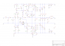
I believe there is a problem with my Vbe resistor values as the driver bases are unbalanced and increase/decrease as a function of the trimpot value.
in a real amp, i do not give too much attention to base voltages,
they are seldom the same any way between npn's and np's...
instead, for as long as i can adjust bias in the vbe multiplier,
and that the output offset voltage is not more than +-100mV,
then you have an amp that is good to go.
of course if you can get the output offset voltage closer to zero, the better....
your amp looks good to me, are you making a board layout?
I would actually get rid of R8 and R17
i agree, not absolutely necessary, but no harm to keep,
let us justt say, optional...
R17 limits collector dissipation in Q9, but it is way too low to matter...
Who is Vallery?............name is Vallery.....
Who is Vallery?
The Russian gentleman who goes by the callsign "vzaichenko". He signed his post with his name a couple pages ago and I misspelt his name in my reply.
Then Vzaichenko is the name used by the Forum and used by all Members. It is unique and definitive.who goes by the callsign "vzaichenko".............
Ranchu32,
i think that by the looks of it you have a circuit that is good to go,
i do not see any major major problem should you decide to go ahead and build it..
I've already built a low-voltage prototype (1pr outputs, 35V rails) using a spare DX Blame MkIII board I have lying around.
I plugged in a speaker and hit the play button on my MP3 player. It plays music and sounds quite good

I'd like to figure out why the output offset (perhaps bad matching of drivers or output transistors?) and then add another two output pairs and crank the rails up to 56V
Last edited:
Member
Joined 2009
Paid Member
ha !- you have sound, very well done !
I have always needed to trim to get small dc offset in the blameless topology, there is always enough mismatch between parts (the LTP, the current mirror, the drivers...) and the most convenient option remains a small trimmer in the current source to the LTP otherwise you'll be fiddling around with different resistor values (which is what I did and hence why I now prefer a trimmer!).
I have always needed to trim to get small dc offset in the blameless topology, there is always enough mismatch between parts (the LTP, the current mirror, the drivers...) and the most convenient option remains a small trimmer in the current source to the LTP otherwise you'll be fiddling around with different resistor values (which is what I did and hence why I now prefer a trimmer!).
ha !- you have sound, very well done !
I have always needed to trim to get small dc offset in the blameless topology, there is always enough mismatch between parts (the LTP, the current mirror, the drivers...) and the most convenient option remains a small trimmer in the current source to the LTP otherwise you'll be fiddling around with different resistor values (which is what I did and hence why I now prefer a trimmer!).
May I ask where you typically insert the trimmer?
ha !- you have sound, very well done !
I have always needed to trim to get small dc offset in the blameless topology, there is always enough mismatch between parts (the LTP, the current mirror, the drivers...) and the most convenient option remains a small trimmer in the current source to the LTP otherwise you'll be fiddling around with different resistor values (which is what I did and hence why I now prefer a trimmer!).
My blameless is now 20 years old.
When I built it, I carefully matched all the components of the diff input pair which needed it. I have never been worried by the DC offset. I checked it just now : less than 2 mV (L) and 1 mV (R) when turning the amp on; after five minutes, both less 1 mV.
Self's amps are conceived to avoid the need of a DC trim pot.
May I ask where you typically insert the trimmer?
That's R7. Should be a series circuit of a fixed resistor (maybe 100 Ohm) + a trim pot (maybe 150 Ohm).
Member
Joined 2009
Paid Member
I will confess that my blameless creations weren't completely blameless, I didn't use a current mirror for balance in the LTP which means more susceptible to dc offset. On the other hand, I've never worried about a bit of dc-offset either - for some folk it's a matter of pride to get it close to zero though.
Moving on up to higher rail voltages it becomes quite important to have good physical mounting of the output devices so that there is good heatsinking. And I also found that it was best to have the Vbe multiplier mounted directly onto the package of one of the power output devices to speed up the thermal control loop. I put the Vbe multiplier onto flying leads from the pcb and then glued it on top of a power device using silicone glue - the glue is good for high temperature and can be removed if the device has to be replaced.
Moving on up to higher rail voltages it becomes quite important to have good physical mounting of the output devices so that there is good heatsinking. And I also found that it was best to have the Vbe multiplier mounted directly onto the package of one of the power output devices to speed up the thermal control loop. I put the Vbe multiplier onto flying leads from the pcb and then glued it on top of a power device using silicone glue - the glue is good for high temperature and can be removed if the device has to be replaced.
And I also found that it was best to have the Vbe multiplier mounted directly onto the package of one of the power output devices to speed up the thermal control loop. I put the Vbe multiplier onto flying leads from the pcb and then glued it on top of a power device using silicone glue - the glue is good for high temperature and can be removed if the device has to be replaced.
That is highly recommended and what I did. Mounting the sensing transistor on the heat sink is very often seen (industrially easier and less costly) but much less optimal.
However, as far as I remember, it has been said here that this works better with TO3 than with "flat" packages like TO220 where there may be some kind of overcompensation.
Last edited:
Member
Joined 2009
Paid Member
You can fine tune the gain of the thermal control loop through the choice of the resistors in the Vbe multiplier if you want. These resistors take current that would otherwise flow through the Vbe transistor and the ratio of the current through the resistors and the transistor can be changed to calibrate it. This is a step beyond what most people do though. At higher rail voltages I really like to know that my thermal control loop is slightly over-compensated rather than under and wouldn't hesitate to place the Vbe device on top of the power device. Others may be less wimpy
Hi all, I have indeed mounted the Vbe transistor on top of one of the TO247 packages using flying leads. The DX Blame board has the multiplier mounted to the heatsink, but I prefer to have it directly on top of a power transistor instead.
I'll post a photo later today to illustrate.
I'll post a photo later today to illustrate.
I've already built a low-voltage prototype (1pr outputs, 35V rails) using a spare DX Blame MkIII board I have lying around.
I plugged in a speaker and hit the play button on my MP3 player. It plays music and sounds quite good
I'd like to figure out why the output offset (perhaps bad matching of drivers or output transistors?) and then add another two output pairs and crank the rails up to 56V
way i see it you have three ways to trim output offset voltage,
1. R7 plus trimpot, like forr said, 100 ohm fixed in series with a 200 ohm trimpot
2. R3 and R4 with trimpot combination, 100 ohm trimpot
3. screening the input tranies Q1/Q2 for good matched vbe at operating currents...
Don't worry about small <10mV output offsets until the driver imbalance has been solved.
The updated sch voltages still show 0mV and 1mV for the driver stopper voltage drops.
These are not acceptable.
I agree, the ~80mV offset at the speaker out is concerning me more than the ~4mV offset at the LTP.
But how do I get more current through the drivers?
I will report back with the voltage drop across the driver emitter resistor, R35.
- Status
- This old topic is closed. If you want to reopen this topic, contact a moderator using the "Report Post" button.
- Home
- Amplifiers
- Solid State
- My Blameless