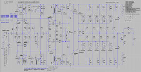
I’ve just put together a full complimentary 200W VFA and would like to hear any comments and opinions. The circuit is nothing new, in fact I would believe others have done this before. Almost all stages are a straight copy from The Book (Cordell’s) with some small difference in details, such as the TMC compensation and the VAS over-current protection. All transistors are from Bob’s model file too.
The entire circuit was rather “carelessly” thrown together and it’s already offering very good promises in performance and stability in simulation (noted in the schematic and the pictures), at least as far as I could tell, especially surprising when I realized all the 2N5401 seem to have twice the Hfe than that of 2N5551. No fancy, advanced techniques or topologies were used or planned to use except a simple beta-enhanced VAS stage.
I will build this amp along side with Dadod’s 200w CFA Vertical MOSFET version and hope mine will be a worthy competitor. My beginner’s worst fear is that there could be fundamental design flaws or big no-noes in the design that I’m not aware of. So I’m putting up the draft here and will appreciate all comments.
Attachments
I’ve just put together a full complimentary 200W VFA and would like to hear any comments and opinions. The circuit is nothing new, in fact I would believe others have done this before. Almost all stages are a straight copy from The Book (Cordell’s) with some small difference in details, such as the TMC compensation and the VAS over-current protection. All transistors are from Bob’s model file too.
The entire circuit was rather “carelessly” thrown together and it’s already offering very good promises in performance and stability in simulation (noted in the schematic and the pictures), at least as far as I could tell, especially surprising when I realized all the 2N5401 seem to have twice the Hfe than that of 2N5551. No fancy, advanced techniques or topologies were used or planned to use except a simple beta-enhanced VAS stage.
I will build this amp along side with Dadod’s 200w CFA Vertical MOSFET version and hope mine will be a worthy competitor. My beginner’s worst fear is that there could be fundamental design flaws or big no-noes in the design that I’m not aware of. So I’m putting up the draft here and will appreciate all comments.
Looks as very nice VFA, complementary IPS, output triple.
Just two things. You have Cordell's book and read the part of indeterminate VAS quiescent currents when current mirrors used in such configuration. Cordell suggested solution in figure 7.10, with R14, R16 resistors.
The triple is prone to instability, you need some kind of compensation there. I used 220pF connected directly between drivers base and collector like in my TT amp, without that amp oscillate even is the simulation does nor show it. Some use the capacitor(or RC combination) to the predrivers.
BR Damir
Why use a very expensive and hard-to-buy 2SC3503C transistor for the bias spreader (Q13)? You don't need exceptionally low Cbc, nor exceptionally high Vearly, nor exceptionally large fT in this position; why not use a 2N2222 (TO-92) or BD139 (TO-126) and save significant money?
Why use low-beta, high-voltage transistors in the current mirrors (Q18,20) + (Q6,17) ?? You know their collectors are hard clamped, guaranteeing VCE < 3 volts at all times {even startup}, so why drop in a 150 volt transistor there? Why not use higher-beta, lower-voltage devices which are optimized not to exhibit quasi-saturation at low VCE? What's wrong with BC327 / BC337?
Why use low-beta, high-voltage transistors in the current mirrors (Q18,20) + (Q6,17) ?? You know their collectors are hard clamped, guaranteeing VCE < 3 volts at all times {even startup}, so why drop in a 150 volt transistor there? Why not use higher-beta, lower-voltage devices which are optimized not to exhibit quasi-saturation at low VCE? What's wrong with BC327 / BC337?
Something I completely don't understand is the position of the Tian probe with TMC.. your placement may not be accurate.
This is a useful place to test. I do not think it is the definitive test.
I am not sure if there is one definitive test for TMC, as there is for Miller, OIC/Cherry and some other schemes.
I believed I had this worked out for TMC too but need to recheck some results.
I knew my answer was not theoretically perfect but expected the inaccuracy would be too small to matter.
Not sure now, so take my previous comments with a bit of salt.
Best wishes
David
I’ve just put together a full complimentary 200W VFA and would like to hear any comments and opinions....
It's an attractive circuit but when I tried it I found the sensitivity to imbalance was not reduced as I expected.
Have you checked this? I only did a quick sim and have not rechecked yet, so I wouldn't swear to it but I would be curious to see your result.
Best wishes
David
Much easier to read if you turn the grid off and use a white field.
Last edited:
Mark, you're right about no point using C3503 as the temp sensor. I confess I was just too lazy not to copy-paste the VAS transistor there. In fact any TO-126 NPN silicon transistor should be good for that job. As about 2N5551/5401 being "wrong" parts for the current mirrors, I use them for the sake of reduced part diversity. You probably also noticed many re-used resistor values, such as 120R, 22R, 470R, 4k7, they are so for the same reason as long as they do not hurt the performance. I believe a short parts list can make PCB assembling work less complicated and can reduce the chance of making mistakes.
Have you thought any about protection systems?
I will use the solid state speaker relay and short-circuit protection in my PCB layout for Dadod's 200W MOSFET CFA AMP. It is in page 38 of that thread, if interested.
It's an attractive circuit but when I tried it I found the sensitivity to imbalance was not reduced as I expected.
Have you checked this? I only did a quick sim and have not rechecked yet, so I wouldn't swear to it but I would be curious to see your result.
Best wishes
David
Much easier to read if you turn the grid off and use a white field.
Dave, thanks for your comments.
It sounds embarrassing but am I right by assuming you are referring to the IPS complementary LTP imbalance? how do you check imbalance sensitivity? I don't think I've done any of that. If I remember correctly you have a write-up/thread about using LTspice. Does it cover the imbalance sensitivity? I'll try searching the forum.
Last edited:
Thanks Dadod!
R73 and R74 in my schematic are the two resistors in Bob's book that help define a stable VAS current. I will reserve base Zobel network components for output and driver transistors in the layout version schematic just like the way I did your CFA layout.
Oh, sorry I did not see those two resistors, David is right about turning off the grid.
I think that you don't need to worry about compensation of the output transistors just do it for the drivers.
.. the IPS complementary LTP imbalance? how do you check imbalance sensitivity?...
I didn't do any very tricky stuff.
I just made one LTP emitter resistor a bit less than the other and checked the current in the VAS, that sort of stuff.
You can make one transistor hotter than the other with a TEMP directive.
Or tweek the BF of one transistor in the pair with a modified model.
Best wishes
David
Last edited:
Hi nattawa, that looks like a pretty good effort.
Just one observation from my side. Putting a decoupling cap next to each output transistor looks like a good idea to conquer ripple e.a. but when the time comes to lay out a PCB it might provide a headache.
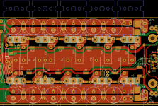
Thank you, ingenieus. Those caps perhaps could be a bit of headache if one insists on single sided PCB. They are not a problem at all for a 2-sided layout, especially if you use SMT parts. Attached is an OPS layout I did for another project that will work with this new Meistersinger amp.
Attachments
.....
Or tweek the BF of one transistor in the pair with a modified model.
Best wishes
David
I'll try that this weekend. Thanks again.
Oh, sorry I did not see those two resistors, David is right about turning off the grid.
I think that you don't need to worry about compensation of the output transistors just do it for the drivers.
Sorry, I did not realize the grid and background would cause grief. The pictures showed up fine on my lower resolution monitor when I previewed the post, even without having my reading glasses on. I do agree a schematic on a white background without grid is a lot more legible, hence my way to go from now on. Thanks for the tip about the drivers.
For a Do-It-Yourself project? Really?... I [reused 5551/5401] for the sake of reduced part diversity. You probably also noticed many re-used resistor values, such as 120R, 22R, 470R, 4k7, they are so for the same reason as long as they do not hurt the performance. I believe a short parts list can make PCB assembling work less complicated and can reduce the chance of making mistakes.
Suppose we are analyzing design option X in a do-it-yourself project. Suppose we believe it has these characteristics:
- Cannot possibly hurt performance in any way
- Likely (but not guaranteed) to improve performance
- Increases assembly time
- Increases the number of different parts, but not the total number of parts
I think of man-hours spent on DIY projects, not as "costs" but rather as "rewards" or "enjoyable hobby time". I don't seek out ways to reduce my time spent in actual construction; a few extra hours (or 20 extra hours) of build-time is, for me, not just acceptable but many times, preferable.
After constructing a few SMD boards, in which I had no choice but to measure each and every (unmarked!) part before soldering it into position, I've come to embrace this approach even in non-SMD applications. It takes an extra 20 seconds to measure a resistor; so if the board has 50 resistors, I'm "wasting" an extra 1000 seconds (17 minutes!) of my life doing these measurements. On the other hand, I get the peace of mind that comes from knowing I'm soldering the right value every single time. And the "cost" is 17 minutes more hobby-time; an easy decision!
I figure that once I've decided to measure every component, there's very little advantage in reducing the number of different component values in the design. Perhaps a price break from ordering qty=50 instead of qty=10, but DIY, for me, isn't about these kinds of cost micro-optimizations.
I feel the same way about active device part-count; to me, the annoyance or burden or risk-of-error from having 10 transistor-types instead of 6 transistor-types, is negligible. I just set out ten egg-cups on my workbench, one per transistor-type, and sort the transistors into the egg-cups. Then, when stuffing and soldering, I extract one from its egg-cup, "measure" it (verify its part# under an illuminated magnifier), and stuff + solder. For a complex project with ~ 36 transistors, this takes an extra 720 seconds (12 minutes) of construction time. I'm happy to spend an extra 12 minutes on my hobby, to obtain peace of mind.
- Status
- This old topic is closed. If you want to reopen this topic, contact a moderator using the "Report Post" button.
- Home
- Amplifiers
- Solid State
- Meistersinger VFA-200, A beginner’s first try in LTSpice