It might be time to put the controversy to "rest'.
The only real way is to actually make some amplifiers.
The best way to start (I might be wrong) , is to assume
that the simulator lies (slightly).
RNmarsh commented that many of his simulated (CFA) amps performed
much better when actually built and I have had VFA's that did not perform
as simulated.
To give everybody some "holiday meat" to chew on ,
the top contenders - that could change .... are posted below.
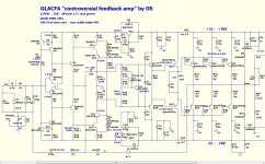
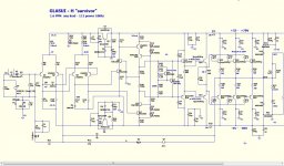
DIYA allows edit of first post ... ALL current work is posted here !
OPS - Amp is split into a output stage/ capacitance multiplier (simple regulator) PCB - 2/3/5 pair versions
are posted - Rated at 70/150/250 watts into 8R. With premium output devices this could be nearly doubled.
Triple output stage topology is used , as well as a 2 device compound thermal compensation circuit.
Similar to the Harmon /kardon 680 -990 series integrated amplifiers.
IPS - Separate small PCB's can plug in to the OPS. All IPS's will run off any supply the
OPS provides. CFA and VFA IPS's can be interchanged ... as the operating voltages
and currents are standardized.
Below is the "lineup" .....
1-3. SLEWMASTER OPS's (V1.2 -3 of them) the "baby" , "master" and monster".
......3 power levels of EF3 goodness. POST(s) #500 , 502 , 504
4. NAD-S-v1.2 IPS (CFA) - Based on the excellent "NX" with servo DC and the
Hawksford Cascode. Member NAF says "it sings" gracefully. Post #518
5. Wolverine-V1.2 IPS (VFA) - "blameless" based with PPM ultra low distortion.
Next logical refinement after the "Badger". POST #599
6. CFA-X and "XH" (CFA , of course) - Similar to the "VSSA/peeceebee" , a very simple amp usable
with the "slew" OPS's. POST #701 -perfected (684 is an error - do NOT use ! )
Edit ... post #2739 is the official schema for the "new" version for CFA-X "H" (hawksford powered).
7. Spookyamp (VFA) Based on the 2500$ Harmon kardon 990 receiver ... uses the classic
Georgia Tech "Leach" topology. Post #803 V1.1 ...
8. Symasui (VFA) - the DIYA "symasym" on steroids post #1628 , almost forgot this one .... Post #1628
9. Kypton-C (CFA) - better CFA-X with servo and super-pair. Post # 4729.
10. Kypton -V (VFA) "classic sansui" 3 stage IPS. Post # 5384.
11. EYESEE (CFA) - IC based amp - alexander amp .....post #4944
12. Kypton ND - (CFA) - best CFA to date ... post # 6782 test - post 6863
More to come ...
ENJOY!
OS
OS
The only real way is to actually make some amplifiers.
The best way to start (I might be wrong) , is to assume
that the simulator lies (slightly).
RNmarsh commented that many of his simulated (CFA) amps performed
much better when actually built and I have had VFA's that did not perform
as simulated.
To give everybody some "holiday meat" to chew on ,
the top contenders - that could change .... are posted below.
DIYA allows edit of first post ... ALL current work is posted here !
OPS - Amp is split into a output stage/ capacitance multiplier (simple regulator) PCB - 2/3/5 pair versions
are posted - Rated at 70/150/250 watts into 8R. With premium output devices this could be nearly doubled.
Triple output stage topology is used , as well as a 2 device compound thermal compensation circuit.
Similar to the Harmon /kardon 680 -990 series integrated amplifiers.
IPS - Separate small PCB's can plug in to the OPS. All IPS's will run off any supply the
OPS provides. CFA and VFA IPS's can be interchanged ... as the operating voltages
and currents are standardized.
Below is the "lineup" .....
1-3. SLEWMASTER OPS's (V1.2 -3 of them) the "baby" , "master" and monster".
......3 power levels of EF3 goodness. POST(s) #500 , 502 , 504
4. NAD-S-v1.2 IPS (CFA) - Based on the excellent "NX" with servo DC and the
Hawksford Cascode. Member NAF says "it sings" gracefully.
Post #5185. Wolverine-V1.2 IPS (VFA) - "blameless" based with PPM ultra low distortion.
Next logical refinement after the "Badger". POST #599
6. CFA-X and "XH" (CFA , of course) - Similar to the "VSSA/peeceebee" , a very simple amp usable
with the "slew" OPS's. POST #701 -perfected (684 is an error - do NOT use ! )
Edit ... post #2739 is the official schema for the "new" version for CFA-X "H" (hawksford powered).
7. Spookyamp (VFA) Based on the 2500$ Harmon kardon 990 receiver ... uses the classic
Georgia Tech "Leach" topology. Post #803 V1.1 ...
8. Symasui (VFA) - the DIYA "symasym" on steroids post #1628 , almost forgot this one .... Post #1628
9. Kypton-C (CFA) - better CFA-X with servo and super-pair. Post # 4729.
10. Kypton -V (VFA) "classic sansui" 3 stage IPS. Post # 5384.
11. EYESEE (CFA) - IC based amp - alexander amp .....post #4944
12. Kypton ND - (CFA) - best CFA to date ... post # 6782 test - post 6863
More to come ...
ENJOY!
OS
OS
Attachments
Last edited:
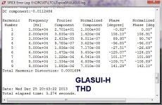
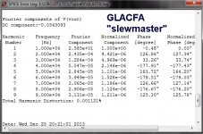
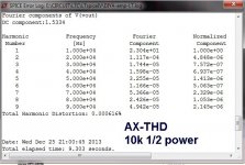
Just a reference - "blameless"
Below is the THD (10k -1/2 power)
of the much abused "blameless" topology.
TMC was used as in the "badger" - not bad
for a simple circuit !
IF .... we go with a modular setup , I will
adapt this to the triple.
It might do better than with the standard
EF2.
All simulations are done with 80mA bias on
the NJWxxxx OP devices.
PS- I will soon adapt the "VSSA" to the hawksford/EF3 ...
it could also be a real contender !
OS
Attachments
Last edited:
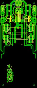
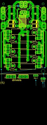
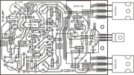
OPS placement.. decisions - decisions
Having the PS in the middle would be worst of 2 "evils".
Having 2 sensitive Vbe's crossing high current returns would
be worse than long traces coming from the fuses (rails) to
supply the regulators (1.) .. in attachment below.
Regulators will have separate decoupling , so this will not matter.
Vbe 1 will attach to the driver heatsink , Vbe 2 will be under the PCB
close to an output.
This is very similar to my HK680 .... even a little better.
As far as grounding ... 1 wire (G2) will run from the input stage star
to the main star. "Star within a star "
Any small signal device will decouple to G2. G1... (the big 'dirty' star)
will only decouple OP devices ,the main rail caps , and the zoble.
I checked the 680 , it also follows these rules.
Also , I am now at 3 pairs for the main OPS.
OS
Having the PS in the middle would be worst of 2 "evils".
Having 2 sensitive Vbe's crossing high current returns would
be worse than long traces coming from the fuses (rails) to
supply the regulators (1.) .. in attachment below.
Regulators will have separate decoupling , so this will not matter.
Vbe 1 will attach to the driver heatsink , Vbe 2 will be under the PCB
close to an output.
This is very similar to my HK680 .... even a little better.
As far as grounding ... 1 wire
(G2) will run from the input stage starto the main star. "Star within a star "
Any small signal device will decouple to G2. G1... (the big 'dirty' star)
will only decouple OP devices ,the main rail caps , and the zoble.
I checked the 680 , it also follows these rules.
Also , I am now at 3 pairs for the main OPS.
OS
Attachments
Member
Joined 2009
Paid Member
Looking good
Thanx ...
While not logged on , I noticed 100's of views/downloads of the "material".
Yours is the first post.
I really want advice , have not built a good CFA yet.
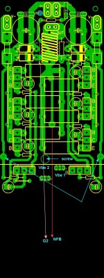
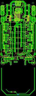
The NFB path can not (should not) "snake" around thesensitive predriver/Vbe area. Shown are the wires (in pink/red - below).
On a double sided PCB one could bring it down along a rail - later date.
Is there a better way ?
Current feedback will "dump" +/- 50ma or more into the clean ground ,
simulation shows to NOT connect to the "lifted" ground directly .... as
you will modulate the 0v reference. With a thick wire between the 2
grounds (G1 and G2) , the reference should be good , even with CF.
This IS NOT an issue with VFA - need a few pointers ....
This is a 1 sided creation for prototypes.
I will keep the big drivers , NJWxxxx is only $.50-75 more than the 15032/
15033. Semitech high current or MJL21193/4 will be options for output devices.
OS
Attachments
.........The NFB path can not (should
I'd put a daughter card to the bottom side of the main PCB, and a string of multiple resistors on it, including the shunt resistor. the sample current can then return right back to the speaker ground terminal. I saw a few suggested it and I tried it in Dadod's 200w CFA SMT layout. Many wont favor this arrangement for obvious reasons, but it seems to be a very quick and clean solution to me.
Member
Joined 2009
Paid Member
Current feedback will "dump" +/- 50ma or more into the clean ground ,
simulation shows to NOT connect to the "lifted" ground directly .... as
you will modulate the 0v reference.
I could wrong (often am) - ultimately I have to think in terms of voltages. The 'error' amplifier of a BJT front-end will receive a control voltage across its base-emitter (this is true whether 'CFA' or 'VFA'). Hence, this BJT 'sees' only a differential voltage and will modulate it's collector current based on the difference in voltage at the base with respect to the voltage at the emitter. If they have different ground references the input error amplifier will not differentiate between the intended signal (feedback & input) and the parasitic signal between the ground references.
And also, although the lifted ground gets modulated by the current, it's linear - since it's lifted with a resistor.
Last edited:
Member
Joined 2009
Paid Member
Member
Joined 2009
Paid Member
Having the PS in the middle would be worst of 2 "evils".
Having 2 sensitive Vbe's crossing high current returns
If you need to compromise in the end due to space, one option is to have small high quality caps local to the output so that high frequency currents are kept to short local loops. Then use larger caps in the middle which will handle lower frequencies - and capacitive coupling of small voltage drops produced by currents flowing in low resistance wide traces to any 'sensitive' traces crossing above will be somewhat ameliorated.
If you need to compromise
(The circuit's) design is enough of a compromise.
Layout is real , I'll make the board 75mm X 200mm... if need be.
OS
Last edited:
Run a wire link on the back of the board for the FB return if you want to keep itThanx ...
I really want advice , have not built a good CFA yet.
sensitive predriver/Vbe area. Shown are the wires (in pink/red - below).
On a double sided PCB one could bring it down along a rail - later date.
Is there a better way ?
OS
separate.
Z
In my nx-Amp layout I just put the FB resistor and gain setting resistors all very close together at the diamond summing junction and ran the connection to THD output as a dedicated track to just before the Zobel (advice from D Self). The clean and dirty grounds are separated by 10 Ohms. I terminated the feedback lower resistor on the clean ground side.
I have no issues with either the nx-Amp or the sx-Amp. Both are exceptionally quiet and sound wonderfully clean and open.
I have no issues with either the nx-Amp or the sx-Amp. Both are exceptionally quiet and sound wonderfully clean and open.
Last edited:
That is what I will do .Run a wire link on the back of the board for the FB return if you want to keep it
separate.
Z
If this turns out good (goes to a PCB house) , a real track will be
added.
OS
In my nx-Amp layout I just put the FB resistor and gain setting resistors all very close together at the diamond summing junction and ran the connection to THD output as a dedicated track to just before the Zobel (advice from D Self). The clean and dirty grounds are separated by 10 Ohms. I terminated the feedback lower resistor on the clean ground side.
I have no issues with either the nx-Amp or the sx-Amp. Both are exceptionally quiet and sound wonderfully clean and open.
I saw Jim's audio NX PCB.
You have the array of resistors in parallel (the divider) near the OPS and
only run the divided Voltage back to the NFB point.
I have a bit more "acreage". My input stage will be inches from any
high current areas .... Capacitance multipliers will be between drivers/ops
and input stage.
Does anyone think 77 X 200mm for the 3 pair or 77 X 250mm for the 5 pair is
too large of a layout.
Once I do the 3 pair layout - I can extend to any mumber of Op pairs in
sprint ... very easy.
OS
Can you put a connector in for a separate front end supply and a jumper to take out the back end...
5 pair is about right and 250mm is great at least for me. Doing it single sided means many can build test and LISTEN.
Already designed cuttable trace/big pads for boosted supplies.
Ground scheme plotted.
Dirty ground - G1 =
Outputs , main decoupling caps ,driver caps, zoble.
Clean ground - G2 =
onboard cap multipliers , Vas load ground , input ground.
PS - Cordell's suggested 50w to-220 feedback resistor is circled in middle (3W or the 50 watter).
OS
Attachments
Last edited:
"You have the array of resistors in parallel (the divider) near the OPS and
only run the divided Voltage back to the NFB point."
It looks like that but they are physically close to the summing junction. The boards are quite small. You have to watch out for capacitance from the feedback junction to ground or across the feedback resistors otherwise you can get gain peaking.
only run the divided Voltage back to the NFB point."
It looks like that but they are physically close to the summing junction. The boards are quite small. You have to watch out for capacitance from the feedback junction to ground or across the feedback resistors otherwise you can get gain peaking.
- Home
- Amplifiers
- Solid State
- Slewmaster - CFA vs. VFA "Rumble"