"Greenamp" was named for using little current. To go SMD , the IPS would be good if it used almost nothing. The slewmaster , with it's EF3 ... allows VAS currents <4ma. The Kypton ND /greenamp even use less if overloaded.
I'm running the greenamp , in normal mode at 14ma current loads. Overload it , it drops to 11ma per rail. Perfect for SMD.
The output stage of the real greenamp will be the only source of heat in the whole circuit. Most of the time , it will act like a small 30W class AB amp running at 20V rails. Pour the wine , crank it up. It will "sip" the 60V rails and put out 100's of watts. A different approach , but the slewmaster IPS's are already designed to accommodate this "better way" (SMD + low current scheme).
OS
Aweful soldering job, sot-223 not even sitting flat, must be a 1st timer. I like smt, I hate throwing all those leads in the trash, wondering how many tons of ore & energy to produce my garbage. start to use FJV992,1845 etc.
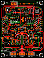
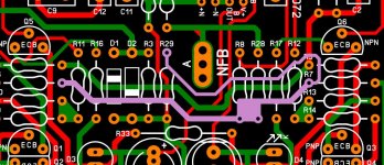
IPS can fit nicely in 100x100mm, the cheap pcb size, OPS have to be much wider and more expensive pcb.
IPS can fit nicely in 100x100mm, the cheap pcb size, OPS have to be much wider and more expensive pcb.
your plans is to have mostly SMD components into the PCB I think that is great is a lot of advantages by doing that way is gonna be plenty of space to work with with the mix of through hole also are you planing to use multilayer?
Vargas
With SMD , a single side can be both the SMD underneath and the through - holes on top ... NEATO !
Aweful soldering job, sot-223 not even sitting flat, must be a 1st timer. I like smt, I hate throwing all those leads in the trash, wondering how many tons of ore & energy to produce my garbage. start to use FJV992,1845 etc.
IPS can fit nicely in 100x100mm, the cheap pcb size, OPS have to be much wider and more expensive pcb.
That was not mine , I can do better even with sot-23 mini's.
What is nice is the matched n/p channel SOT for differentials.
They are even thermally connected. Offset will be minimized.
A dual differential will fit in a square centimeter.
OS
what, you do not have any of your smt work to show us ")
This IPS design lends itself well to smt when I see the long runs going across the pcb, you will need lots of vias, but drill hits are free.
look at IMX8, IMT4, common sot-26 along with the DMMT5551_5401
It is funny that all the good Nichicon ecap models are still THT.
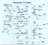
Can you post the updated .asc file V1.2?
The glue,place,cure,wave process.With SMD , a single side can be both the SMD underneath and the through - holes on top ... NEATO !
This IPS design lends itself well to smt when I see the long runs going across the pcb, you will need lots of vias, but drill hits are free.
look at IMX8, IMT4, common sot-26 along with the DMMT5551_5401
It is funny that all the good Nichicon ecap models are still THT.
Can you post the updated .asc file V1.2?
Last edited:
ugly jumper be gone!
hello guys man finally I was able to remove those ugly pads that I was thinking that they be ok but no enough for me I stay on it till a figure it out on how to remove them yes sir
hello guys man finally I was able to remove those ugly pads that I was thinking that they be ok but no enough for me I stay on it till a figure it out on how to remove them yes sir
Attachments
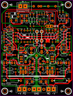
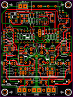
C11,12 could be moved right beside the power pins of U1. The rule of supply filtering is to have the feed go to the cap then a very short trace/stub, on the same layer(smt), to the device power pins. TL074 are pretty forgiving, so your placement would work, a faster opamp might have issues. this is an integrator, so it has lots of AC feedback.
What computer operating system are you using?
I'll see if I have the time to go over the opamp wiring.
What computer operating system are you using?
I'll see if I have the time to go over the opamp wiring.
oh I'm uisng Windows 10 64bit OS
Oh ,no M$ owns greenamp.
OS
While you are at it, rotate R29, 90 degree CW, put above R33, shortens that trace from R7, will have to move parts above up some, but I see room
TO-92 footprint could be all pins in straight line, 100 mil lead spacing since these parts come on paper tape with that lead forming i.e KSC1845FTA, BC560CTA
The U1 wiring looks to be correct.
TO-92 footprint could be all pins in straight line, 100 mil lead spacing since these parts come on paper tape with that lead forming i.e KSC1845FTA, BC560CTA
The U1 wiring looks to be correct.
Last edited:
- Home
- Amplifiers
- Solid State
- Slewmaster - CFA vs. VFA "Rumble"