Member
Joined 2009
Paid Member
(edit)
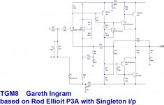
Note - what started out as an attempt to evolve the p3a has ended up as a complete redesign of every stage. This amplifier is my best. Anybody wanting to build this amp for DIY purposes (only) should find all they need in this thread.
Some useful posts:
#232 - discovery that dual colour LED has insufficient headroom for the ‘green’ side to work (my fix is on #314)
#238 & #242 - discovery of, and changes to deal with cross-conduction at v. high frequencies
#314 - fix to pcb for very first incarnation (corrected on subsequent pcb layouts)
#407 - pcb files and (a now old) bill of materials
#597 - a bill of materials for Mouser
#604 - my as-built schematic (with C3 shown wrong way around, should be installed + terminal to ground)
#632 - a comment on bias for the output (60mA) note original pcb has a silkscreen error with the bias and dc offset adjust labels swapped around
#645 - a note on correct orientation of C3 (shown wrong way on pcb silk screen)
#768 - some photos and comments on how the power devices mount under the board and the use of some TO-126 transistors with legs removed are used as 'spacers'
#772 - some photos and comments on incorporating an output inductor into the wiring
#950 - updated bill of materials (BOM) based on Digikey.ca
#994 - spice file for the amplifier
#1131 - KiCad files from 'longface54'
#1215 - updated KiCad files from ‘jpk73’
Builders: Go slow, solder all the small parts first and clean off the flux before moving on. Read the thread, I know it's long but there's advice in there for you.
Builders Comments:
'Ranchu32': "this is a fabulous amp; one of the best. I love the sense of energy and the dynamic performance, which I feel is somewhat lacking in the basic P3A. But it loses none of the P3A's best qualities: that beautifully smooth and detailed midrange, and crystal clear highs." "the more time I spend with TGM8 the more impressed I am. Having now heard the VSSA, I am equally impressed and it is deserving of the high praise it is getting around here. But your design is in the same league: similar in many respects and subtly different in others. I suspect TGM8 will better suit my tastes"
'Lordearl': "As to the sound - phenomenal, incredibly relaxed, yet still highly detailed! Tempted to use the good channel on my better speakers just to enjoy it for a while! A very inviting sound for sure." "My initial impression (mono only) is the same, the low frequencies are crisp and punchy - never heard anything quite like it. The treble easily rivals my 6L6 ultra linear push pull amp with Tango output transformers, plenty of air, no fatigue (also no apparent dumbing down of the sound!). Makes you realise why you loved audio in the first place!"
'still4given': "You done good Gareth! I can see why you were so satisfied. I've got some Gerry Mulligan playing through it right now and it is beautiful. Thanks for sharing this with me." "It really is very nice sounding. Seems as good as the VSSA and that is one fine sounding amp."
'pronk': "I originally planned to build just two boards but liked the TGM8 so much that I built six (four to power my LXmini and two for my home office). Note these boards are densely populated and have about 30 SMD components. This is probably not something you can throw together in an evening. The end result is definitely worth the effort. This is one of my favourite amplifiers. Sound quality, particularly bass, is excellent. I appreciate the built-in speaker protection which makes this amplifier more of a complete product safe to use with expensive speakers."
'RCruz': "Finally had the opp to listen to it and i am really pleased with the sound...the best bass grip I heard in years"
'auriga2001in': "Thanks for the wonderful amp. I have two amps (BJT, Latfet outputs) running wonderfully for a year now."
'pinnocchio' "This amp has some really good grip on the bass driver, very fast and precise. I haven't done all the tests yet but looking very good so far."
‘Do’: “Amps are working perfectly. I truly love the bass from this amplifier, very hard to believe until you hear it! Solid, in control of the speaker, I mean just perfect!”
'audiorasp': "I really like these amps! They have been powering my LX521's for about month now and I find their presentation to be detailed and powerful, but in a relaxed way, if that makes sense."
'longface54': I decided to go for it. I had some PCBs made, using the published gerbers, and built two amps. Powered each one up on the lab PSU and, bingo! They both worked first time and the DC offset and bias was very stable... Right away the sound had such authority and pace but in a relaxed and musical way with a softness in the upper registers. ... I’m listening as I write so I’m off to turn the volume up... just a little.
’jpk73’: I connected my speakers and played some music: excellent!!! I am very happy") .
.
Also - I can not edit attachments to the first post, the schematic you see in this first post shows my initial scrawl - not to be confused with the schematic of the as-built amplifier.
Note - what started out as an attempt to evolve the p3a has ended up as a complete redesign of every stage. This amplifier is my best. Anybody wanting to build this amp for DIY purposes (only) should find all they need in this thread.
Some useful posts:
#232 - discovery that dual colour LED has insufficient headroom for the ‘green’ side to work (my fix is on #314)
#238 & #242 - discovery of, and changes to deal with cross-conduction at v. high frequencies
#314 - fix to pcb for very first incarnation (corrected on subsequent pcb layouts)
#407 - pcb files and (a now old) bill of materials
#597 - a bill of materials for Mouser
#604 - my as-built schematic (with C3 shown wrong way around, should be installed + terminal to ground)
#632 - a comment on bias for the output (60mA) note original pcb has a silkscreen error with the bias and dc offset adjust labels swapped around
#645 - a note on correct orientation of C3 (shown wrong way on pcb silk screen)
#768 - some photos and comments on how the power devices mount under the board and the use of some TO-126 transistors with legs removed are used as 'spacers'
#772 - some photos and comments on incorporating an output inductor into the wiring
#950 - updated bill of materials (BOM) based on Digikey.ca
#994 - spice file for the amplifier
#1131 - KiCad files from 'longface54'
#1215 - updated KiCad files from ‘jpk73’
Builders: Go slow, solder all the small parts first and clean off the flux before moving on. Read the thread, I know it's long but there's advice in there for you.
Builders Comments:
'Ranchu32': "this is a fabulous amp; one of the best. I love the sense of energy and the dynamic performance, which I feel is somewhat lacking in the basic P3A. But it loses none of the P3A's best qualities: that beautifully smooth and detailed midrange, and crystal clear highs." "the more time I spend with TGM8 the more impressed I am. Having now heard the VSSA, I am equally impressed and it is deserving of the high praise it is getting around here. But your design is in the same league: similar in many respects and subtly different in others. I suspect TGM8 will better suit my tastes"
'Lordearl': "As to the sound - phenomenal, incredibly relaxed, yet still highly detailed! Tempted to use the good channel on my better speakers just to enjoy it for a while! A very inviting sound for sure." "My initial impression (mono only) is the same, the low frequencies are crisp and punchy - never heard anything quite like it. The treble easily rivals my 6L6 ultra linear push pull amp with Tango output transformers, plenty of air, no fatigue (also no apparent dumbing down of the sound!). Makes you realise why you loved audio in the first place!"
'still4given': "You done good Gareth! I can see why you were so satisfied. I've got some Gerry Mulligan playing through it right now and it is beautiful. Thanks for sharing this with me." "It really is very nice sounding. Seems as good as the VSSA and that is one fine sounding amp."
'pronk': "I originally planned to build just two boards but liked the TGM8 so much that I built six (four to power my LXmini and two for my home office). Note these boards are densely populated and have about 30 SMD components. This is probably not something you can throw together in an evening. The end result is definitely worth the effort. This is one of my favourite amplifiers. Sound quality, particularly bass, is excellent. I appreciate the built-in speaker protection which makes this amplifier more of a complete product safe to use with expensive speakers."
'RCruz': "Finally had the opp to listen to it and i am really pleased with the sound...the best bass grip I heard in years"
'auriga2001in': "Thanks for the wonderful amp. I have two amps (BJT, Latfet outputs) running wonderfully for a year now."
'pinnocchio' "This amp has some really good grip on the bass driver, very fast and precise. I haven't done all the tests yet but looking very good so far."
‘Do’: “Amps are working perfectly. I truly love the bass from this amplifier, very hard to believe until you hear it! Solid, in control of the speaker, I mean just perfect!”
'audiorasp': "I really like these amps! They have been powering my LX521's for about month now and I find their presentation to be detailed and powerful, but in a relaxed way, if that makes sense."
'longface54': I decided to go for it. I had some PCBs made, using the published gerbers, and built two amps. Powered each one up on the lab PSU and, bingo! They both worked first time and the DC offset and bias was very stable... Right away the sound had such authority and pace but in a relaxed and musical way with a softness in the upper registers. ... I’m listening as I write so I’m off to turn the volume up... just a little.
’jpk73’: I connected my speakers and played some music: excellent!!! I am very happy
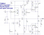
. Also - I can not edit attachments to the first post, the schematic you see in this first post shows my initial scrawl - not to be confused with the schematic of the as-built amplifier.
Attachments
Last edited:
Member
Joined 2009
Paid Member
I forgot to mention another key thing about the input stage. By controlling the d.c. level in the feedback network in this way, the feedback capacitor is quickly brought up to the correct bias voltage and doesn't create the turn-on issues normally associated with a Singleton input. There are other contributions to the turn-on behaviour of the P3a and this is something I still have to look at.
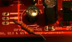
PCB ? --- I'm afraid my recent designs have been unpopular around here because I make use of a mixture of through-hole and surface mount. Some people really are still afraid, in this day, of surface mount. My plan so far on my TGM7 has worked fairly well. I use through hole for parts with 3 or more connections such as transistors and trim-pots. I use through hole parts for all large capacitors too. Where I have been using surface mount is for resistors and even then I use 1206 sized parts. These are parts are big enough to read their labels so you can read off the values of them. Have a look at the attached photo to see a through hole resistor lying on top of a pcb near a surface mount resistor. It's not hard to use at all, a pair of small pliers to hold it in place whilst you solder one end at a time. You end up being able to solder them in quickly and easily, with little solder. They allow for shorter signal traces and more compact design which can be very handy when your feedback amplifier has open loop unity gain in the MHz region. The only disadvantage is that you can't easily remove surface mount resistors unless you have two soldering irons, or be prepared to crack it and remove it in two pieces. I haven't decided which approach to designing the pcb to take with TGM8 yet.
PCB ? --- I'm afraid my recent designs have been unpopular around here because I make use of a mixture of through-hole and surface mount. Some people really are still afraid, in this day, of surface mount. My plan so far on my TGM7 has worked fairly well. I use through hole for parts with 3 or more connections such as transistors and trim-pots. I use through hole parts for all large capacitors too. Where I have been using surface mount is for resistors and even then I use 1206 sized parts. These are parts are big enough to read their labels so you can read off the values of them. Have a look at the attached photo to see a through hole resistor lying on top of a pcb near a surface mount resistor. It's not hard to use at all, a pair of small pliers to hold it in place whilst you solder one end at a time. You end up being able to solder them in quickly and easily, with little solder. They allow for shorter signal traces and more compact design which can be very handy when your feedback amplifier has open loop unity gain in the MHz region. The only disadvantage is that you can't easily remove surface mount resistors unless you have two soldering irons, or be prepared to crack it and remove it in two pieces. I haven't decided which approach to designing the pcb to take with TGM8 yet.
Attachments
Last edited:
Smd 1206 size resistors are quite easy to solder and desolder if one uses a magnifying lamp. I put some solder on one pad, then put the resistor in place and hold it until the solder cools, 1-2 seconds. Easy to do the other side as the resistor is held in place by the first solder. Desoldering with braid is pretty much the reverse of the above. It's possible to save a desoldered resistor, but they are so cheap that I usually use new ones.
For me, using the magnifying lamp is essential and I now use it for all soldering.
For me, using the magnifying lamp is essential and I now use it for all soldering.
Member
Joined 2009
Paid Member
Output Stage - I want to preserve the sound signature, so we keep the simple CFP and most likely with BD139/140 and 2SC5200/2SA1943 pairings. I will look at alternative drivers but this is a good as any place to start.
Trouble is that with higher rails/powers and more difficult loads we start to run out of steam with a single pair of outputs. The input impedance of the power devices drops at high current (so called beta droop) which taxes the drivers. In the CFP the drivers feed the base of the output devices with their collectors - a high impedance drive. This is the worse case for driving power BJTs at high currents with beta-droop. Even the venerable 2SC5200's have some fall off in beta at high current. The other issue is BJTs are easily destroyed if over-stressed. The solution is usually to add another pair of outputs.
There have been CFP output designs with more than one pair of outputs, some use one driver per pair of power devices, others have a separate dedicated driver per power device so a pair of outputs needs two drivers. I remember Sakis saying that none were quite as successful as the single output pair. So I'm keeping to the single output pair.
However - by adding a pair of power MOSFETs that only turn-on when the power BJTs reach high current we can divert the extra load current away from the BJTs and cap the maximum current flow through them. Under difficult load conditions or peak powers the MOSFETs will take on the additional stress and protect the BJTs. These MOSFETs are more robust and do not have beta droop. Since the MOSFETs remain off during low-medium powers they do not contribute to the sound of the output stage for normal listening (whatever that is).
So we preserve the sound of the single output pair at low-to-medium powers but enable the amplifier to drive higher peak powers into more difficult loads when needed
Attachments
Last edited:
Gareth,
Clever approach.
The mosfets saturate much further from the rail than the bipolars. You could be in a situation where the bipolar is approaching rails, but when the mosfet cannot turn off because the gate drive is too close to the rails.
How about substituting the devices so that at lower output the mosfet operates and at high output the bipolar chimes in to help? Would this work?
Hugh
Bigun, I'd be really interested in putting this up against my P3A that I recently built. Hopefully someone produces some boards (either SMT, TH, or a mixture - doesn't bother me).
Is there much difference between the SC1943/5200 and Motorola silicon? Reason being I have a small stockpile of MJL4281/4302/3281/1302 devices.
I prefer the simplicity of the first version without the MOSFETS in the OPS. 50wpc is a useful amount of power.
Is there much difference between the SC1943/5200 and Motorola silicon? Reason being I have a small stockpile of MJL4281/4302/3281/1302 devices.
I prefer the simplicity of the first version without the MOSFETS in the OPS. 50wpc is a useful amount of power.
I notice you have added R-C filters for the VAS and OPS, but omitted the filter caps and 100nF decoupling caps on the OPS rails. Was that intentional?
Another request:
When you produce the boards can you make it a stereo layout with bulk caps onboard? This circuit has a very low parts count so should be possible, whilst keeping the circuit board fairly small, particularly if SMT components are utilised
Another request:
When you produce the boards can you make it a stereo layout with bulk caps onboard? This circuit has a very low parts count so should be possible, whilst keeping the circuit board fairly small, particularly if SMT components are utilised
Member
Joined 2009
Paid Member
Hi All,
PCB - well I'm still deciding on the approach. It's primarily for my project rather than public use so I can't promise it will please all.
The schematic I posted is a simplified layout - there will be additional parts. I haven't looked at the VAS yet and if I stay with a simple VAS I will include footprint on the PCB for two-pole compensation and phase lead compensation along with bypass caps on the rails.
Hugh - I will give some proper thought to your suggestions for sure.
One thing to note, the pin-out for the MOSFET and the power BJT are almost inter-changeable (gate-drain-source usually maps onto base-collector-emitter) allowing a 'universal' layout and experiments to follow.
Member
Joined 2009
Paid Member
Is there much difference between the SC1943/5200 and Motorola silicon? Reason being I have a small stockpile of MJL4281/4302/3281/1302 devices.
I believe these devices of yours are very good and should work just as well although I haven't used the MJL4281 myself.
When you produce the boards can you make it a stereo layout with bulk caps onboard? This circuit has a very low parts count so should be possible, whilst keeping the circuit board fairly small, particularly if SMT components are utilised
That's an interesting idea, I know Hugh likes this approach. I'll give it some thought to see if it will suit what I have in mind but the freeware version of Eagle layout software I use may not allow a large enough PCB for it all. I was thinking of a compact mono board (that could be used in a multi-channel amplifier) with solid-state dc-protection on the same board as an integrated unit - would this be appealing ?
Last edited:
I was thinking of a compact mono board (that could be used in a multi-channel amplifier) with solid-state dc-protection on the same board as an integrated unit - would this be appealing ?
Sure would be - and I notice there's a few other Aussies interested in this thread, happy to assist in coordinating the dispersal of some PCBs downunder if the project gets under way...
Onboard DC protection would be appealing, as would anything else that results in greater integration. I prefer to use large 30A relays that can reliably handle the breaking current. PCB types that carry this rating are quite bulky so you could keep them off-board and integrate just the trigger logic. These components are compact and wouldn't add much to the overall board size, and could easily bypassed if the constructor didn't want the protections.
If it has to be a mono design, could you please also consider incorporating the filter caps also. If space constraints are an issue, a small amount of capacitance could be accomodated, which constructors could augment with off-board caps as desired.
If it has to be a mono design, could you please also consider incorporating the filter caps also. If space constraints are an issue, a small amount of capacitance could be accomodated, which constructors could augment with off-board caps as desired.
1206 SMD resistors seem big enough for older diy-ers to work with.
I also think that the circuit will work fine with higher rails voltage, two pairs of output BJTs and single drivers (if high power is really needed). The proof is LJM L12 amp that Ian Finch built.
Also, the circuit may be tried with only one pair of MOSFET outputs, but CFP output configuration should remain.
Last edited:
Member
Joined 2009
Paid Member
What about the VAS ? - is it important to leave this alone so as to retain the character of the P3a. We could allow for an option on the PCB for an enhanced VAS so that we don't have to change it, but we could still try an enhanced VAS and keep it only if we wanted. The penalty is space on the pcb.
What I had in mind, in the full spirit of the P3a, was a CFP based VAS. Why might we consider this ?
- It should be more linear, especially at lower frequencies and large signals. At higher frequencies the simpler single VAS device is partly linearized by Cdom, which takes signal from the collector and feeds it back to the base.
- The P3a does not have a class A emitter follower buffer driving the output devices, the drivers also switch off with the outputs which puts some switching noise right back at the VAS. A CFP VAS will provide a buffer.
- We could get fancy and use a CFP VAS to bootstrap the input, this would get us another 10dB of open loop gain (I did this in my TGM6 amplifier - thread around here somewhere) and it works well.
Thoughts ?
I've tried some of the ideas suggested here on the P3a. One I spent some time on, was increasing the number of output devices. I was still using MJ15003/4 at the time and these are quite different to modern triple-diffused and LAPT transistors that are more flexible in application, due to their higher Hfe, Ft and lower capacitance.
It seems that with a compact layout, you can preserve CFP stabilty without needing lots of base stoppers, ferrite beads or bypassing to squish signs of oscillation. However, my version that used MJ15003/4 in virtually just a paralleled output stage with 4.7R stoppers, sounded less like a P3a and more like other old DIY designs from the 1970s. I think Sakis was right in his conclusion about adding more output devices but I regret not having access to an analyser to see what had actually changed to spoil it. That would be an interesting study, whether drivers, load, matching etc. with implications for many other designs too. Given that when we add more devices for more power but really, still use the amplifier at a tiny 1-5W in typical domestic use, we do change the operating conditions and usually, the bias too.
I suspect that when there is noticeable crossover distortion, adding more devices adds more distortion products - given the same device operating conditions. Of course, if you only simulate results using identical models, you may not notice what more likely happens in real life, where individual device physics will all differ to some degree, as will their distortion products - which become massive in quantity with IMD, the higher in frequency you look.
I don't think, when based on bootstrapped capacitor VAS design, that linearity is the order of the day with P3a. I'd say that even-order non-linearity was the aim, without hesitation. I have my doubts about the significance of a CFP VAS to the spirit of the P3a or a benefit but then, its your project - only my
- Home
- Amplifiers
- Solid State
- TGM8 - my best amplifier, incredible bass, clear highs, no fatigue (inspired by Rod Elliot P3a)