I have create the schematic for the power supply include several voltages and current flows (measuring include the preamp devices in operating mode).
Philips starts a "Consistent Global Presence" (actually a slogan) in the 90’s:
“Let’s make things better”
I now have the same train of thought.
Some choices of transistors for me are suspect resp. incomprehensible in order to the necessary current head room. Particularly the 2N3055 and MJ2955.
Whether too much whiskey bottles could have been present during the circuit design?
Therefore the question:
How can one make things better ?
Thanks for advices.
Great, many thanks!
On page 52 of the article, the author was surprised the voltage regulators did not use the usual loop feedback for regulation; which is the case here. He suggested a capacitance multiplier instead; maybe the cap [100 uF] on the output of LM334Z at the base of 2N3440. Also, the author said the dual PSUs are stacked [as shown], and use the same rather than complementary components; like dual PSUs using uA723. He thought this is is beneficial.
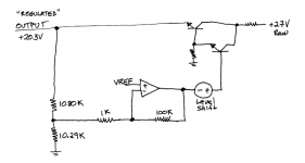
Thank you for the analysis.Gosh, that 100K resistor lowers the gain of the NFB path (from Vout to Darlington base) to about eight: [-7.72 according to SPICE]. The power supply's closed loop output impedance will be high but extremely wideband. Original!
Hello Mark. Is it possible that the 100 uF capaciance of the cap in the level shifter is also multiplied by the gain of the compound bjts? If yes, then this regulated PSU used a limited NFB plus capacitance mutiplication; a best of both worlds.Gosh, that 100K resistor lowers the gain of the NFB path (from Vout to Darlington base) to about eight: [-7.72 according to SPICE]. The power supply's closed loop output impedance will be high but extremely wideband. Original!
Thanks for your reply.You could analyze the circuit manually (by writing the equations), or put it into LTSPICE, or both. In this case, they give the same answer.
For me the PSU schematics look pretty nice. Especially the trick to use the first power transistor to drive the second one, this increases overall current gain by at least 2x, without an extra transistor. Reminds me a lot of some tricks IC designers are playing in bipolar processes ...
Andreas, as you probably may know, I have access to a 20W Yttrium Fiber Laser with galvo, which I already used to burn away the epoxy of QFN chips down to the upper metal layers (leaving even the golden bond wires intact !!). Unfortunately this doesn't stop at plastic transistor`s epoxy housings or on PCB epoxy, but easily on metal ...
But in case one would erode a rectangular hole down on the potting side of such a module, one could probably go down easily to the bottom copper layers of the PCB (in case the parts are on the other side). Then (hopefully) isolate the defective part, interrupt it's traces and connect a replacement on the back side and pot everything together again ... voilà ... simpliste n'est pas !?
I expect that Laser ablation would need about 5..10minutes per mm at the footprint of a matchbox ... I would try ...
Last edited:
For me the PSU schematics look pretty nice. Especially the trick to use the first power transistor to drive the second one, this increases overall current gain by at least 2x, without an extra transistor. Reminds me a lot of some tricks IC designers are playing in bipolar processes ...
Andreas, as you probably may know, I have access to a 20W Yttrium Fiber Laser with galvo, which I already used to burn away the epoxy of QFN chips down to the upper metal layers (leaving even the golden bond wires intact !!). Unfortunately this doesn't stop at plastic transistor`s epoxy housings or on PCB epoxy, but easily on metal ...
But in case one would erode a rectangular hole down on the potting side of such a module, one could probably go down easily to the bottom copper layers of the PCB (in case the parts are on the other side). Then (hopefully) isolate the defective part, interrupt it's traces and connect a replacement on the back side and pot everything together again ... voilà ... simpliste n'est pas !?
I expect that Laser ablation would need about 5..10minutes per mm at the footprint of a matchbox ... I would try ...
Thank you - interesting considerations.
Next step will be to create drawings from the motherboard circuit of my currently present C1 device.
Follow PCB version it is: PN 58616 Rev. C.1
This preamp PCB runs with +/- 20V3
the presently available schematics in Germany are follow (according the numbering on the schematics itself):
1) COHERENCE ONE MOTHERBOARD with use of +/-49VDC without revision numbering
Date: 6-Jun-2002
File: C:\Data\..\PN 58616 - C1 Motherboard.Sch Drawn By: Rich Maez
2) COHERENCE ONE MOTHERBOARD with use of +/-51VDC
Date: 3-Dec-2002
File: C:\Data\..\PN 58616 - C1 Motherboard, Rev. A S/N 001 to 125
Thus both schematics are not helpful for me. Additional there are no values and types to read for the devices - nevertheless there is to read on the incomplete drawing papers "strictly confidential - not for release" (written by hand with a marker pen in red color).
In the moment I am very confused.
For me rises up follow important question:
How many different versions are there at whole from this preamp model?
According the now presently informations there may be 7 different versions:
1) First revision without numbering (fact according presently schema) for +/-49VDC
2) Rev A S/N 001 to 125 (fact according presently second schema) for +/-51VDC
3) Rev A.1 S/N above 125
4) Rev B
5) Rev. B.1
6) Rev C
7) Rev C.1 (fact according exist PCB from preamp device with S/N 000614 for +/-20VDC)
Are my estimates concerning 2) to 6) correct ?
If yes, how many different potted devices are there at whole (please note: 4 different pieces for each revision !!!) ?
It seems to have a problem similar to Electrocompaniet's power amp AW100 (Ampliwire 100) from which it was known, that there are also many different versions on the marked - go to
http://www.diyaudio.com/forums/soli...wire-100-aw-100-aw100-different-versions.html
From two versions I have detailled schematics from Electrocompaniet itself and from one (mor new) version an own drawing.
From JRDG actually I have nothing.
Hello tiebassuebertr. Found the attached schematic of a high performance ac op amp in a 1975 Audio magazine.maybe a replacement for pottet stuff:
Burson DIY & Upgrades
Attachments
interesting paper - thank you very much.Hello tiebassuebertr. Found the attached schematic of a high performance ac op amp in a 1975 Audio magazine.
the schematic of this preamp is further completed and additional questions rises up:
1) There are unknown devices, maybe suppressor diodes. Who know, what it is (I use a symbol for a varactor diode -this diodes are to see at second picture from post #2, main PCB left corner, in front of "PHONO AMP HIGH LEVEL" - module resp. left hand from DIP-8 socket)?
2) in one of the regulators (for phono high level, left CH) a 750 ohms resistor isn't in use. Are therefore a special reason possible?
3) in one of the regulators (phono, low level) the input HF cap for the pos. voltage input has an other value: 470nF instead usual 47nF. That means this (go to post #2 for looking - first image shows this big orange colored foil cap on the right hand outer edge of the main PCB and second image on the left hand side) ?
Thank you for your advices.
Attachments
Last edited:
The schematic puzzles me in (at least!) two places.here now the schema of the signal gain stages (phono/RIAA and line amps).
- Very low resistance (511R) between servo-out and feedback node
- No NFB from output to input of servo 1st stage; 1M resistor does nothing
The 33nF capacitor (RIAA equalization?) directly shorting the output of the 1st forward path gain block to ground, might offer a hint about its internal architecture. VCCS? VCVS? CFB? etc.
Attachments
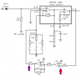
The schematic puzzles me in (at least!) two places.See arrowheads in attached schematic. (I removed some clutter)
- Very low resistance (511R) between servo-out and feedback node
- No NFB from output to input of servo 1st stage; 1M resistor does nothing
The 33nF capacitor (RIAA equalization?) directly shorting the output of the 1st forward path gain block to ground, might offer a hint about its internal architecture. VCCS? VCVS? CFB? etc.
Hello Mark. I find the circuits uncovered by Andreas quite interesting. My impressions which track your concerns above are:
- The resistance [511R] is in parallel with that engaged by one closed switch [or none]. The resulting equivalent resitance determines the voltage gain of the 1st gain stage of the module per the standard equation[1+Rf/Requiv].
- The first OA of the dc servo is operating open loop, and in the inverting mode. The 1 Meg converts voltage at the module's output to current so as to bias the non-inverting port. I can also imagine a ten or higher Meg resistor between the output and inverting ports from /due to leakage between the pcb traces so as to close the loop instead.
- The second OA of the dc servo is operating as an inverter with a gain of -1; plus the function of a low pass first order filter.
- The net phase due to the servo OAs in non inverting. The first stage of the gain module provides the needed phase inversion [reversal of dc] because the dc servo output via 511R feeds its inverting port.
- Amazing the servo loop is stable, and must give tight servo or zero dc [no loose+/- millivolts] at the output of the gain module.
Your analysis makes full sense; thanks. I should have remembered; because I've used this classic [integrator] circuit in projects for dc servo'ing.The missing circuit element in the servo first stage, is the integration capacitor. Maybe it's hidden behind something or under something, on this PCB.
Bob Cordell's book, p.160 (Figure 8.5) shows an example schematic.
The schematic puzzles me in (at least!) two places.
See arrowheads in attached schematic. (I removed some clutter)
- Very low resistance (511R) between servo-out and feedback node
- No NFB from output to input of servo 1st stage; 1M resistor does nothing
The 33nF capacitor (RIAA equalization?) directly shorting the output of the 1st forward path gain block to ground, might offer a hint about its internal architecture. VCCS? VCVS? CFB? etc.
Thank you for your advices in this schematic.
Many errors are still present. It is a mixture between several design errors from Rowland itself and my own drawing errors.
The missing resistor I have overlooked - there is a associated place present (two pieces through hole solder eyes/each resistor) - OTOH - the resistor isn't equipped (NU means "Not in Use").
The 511R resistor has the correct value according PCB - but please note: the offset servo ICs are also not in use, only the sockets are present.
I doubt, that the 33nF capacitor (RIAA equalization?) does directly shorting the output of the 1st forward path gain block. My estimate is the use of an internal additional serial resistor (like at the second filter part for RIAA - where this resistor is outside).
I does provide additional errors while drawing, which I have found by a closer look:
1) all 750 R and 510 R resistors at input and output have a value of 150R.
2) the 1K12 resistor at the second RIAA part has a correct value of 1K18 (1180 ohms).
A re-inspection after a longer break is likely to stimulate additional own drawing errors.
Last edited:
first update of the schema in the attachment.here now the schema of the signal gain stages (phono/RIAA and line amps).
No informations concerning post #53? Particularly to my first question?
On the unknown devices I read follow:
UZ
104
M
50V
Are this supressor diodes?
Attachments
Last edited:
- Home
- Amplifiers
- Solid State
- Jeff Rowland Coherence 1 - Schematic for the Modules wanted