Bom or instructions?
In the first post there is index list and no. 7 is for 200W CFA with or without balanced board.
There some small differences, there is no screen error any more on the new 200W amp board and one more resistor on balanced board. I will prepare the list of that small differences soon before the PS boards arrive, expected next week.
Damir
")
All boards will be here this week and I will send PayPal money request. All from the list, please PM your PayPal email address.
200W amp board order list
………………………………………………………………..confirmed
tjencks 6 pcs 200W amp boards...………..OK
vitalica 2 pcs 200W amp boards …………..OK
malibutwins 2 pcs 200W amp boards.....OK
arthur 4pcs 200W amp boards...…………….OK
zsaudio 2pcs 200W amp boards...………...OK
PS regulator board order list:
Arthur PS regulator board 4pcs...….OK
zsaudio PS regulator board 2pcs.....OK
mlloyd1 PS regulator board 2pcs.....OK
Vitalica - PSU PCB 2 pcs ....OK
tjencks- PSU regulator board 6pcs....OK
Lbud4- PSU regulator board 2pcs......OK
malibutwins-PS regulator board 2pcs....OK
balance in board order list:
Arthur- balance inputs board 4pcs ... ... .OK
Vitalica - balance inputs board 4pcs .... OK
-----------------------------------------------------------------
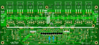
Short recapitulation about 200W CFA balanced ready board.
1. It's possible to use it in pure CFA mode (unbalanced input), and in this case small FB board is used with 8 1k1 2W 1% resistor on it. They are connected four parallel in series with other four in parallel.
2. If small balanced add board is used the amp act as VFA with balanced inputs. From 200W CFA VMOSFET BOM is clear what components not needed to be soldered on the main amp board
3. PS regulator needs +-70V input to get +-65V output.
If I missed something please don't hesitate to ask.
200W amp board order list
………………………………………………………………..confirmed
tjencks 6 pcs 200W amp boards...………..OK
vitalica 2 pcs 200W amp boards …………..OK
malibutwins 2 pcs 200W amp boards.....OK
arthur 4pcs 200W amp boards...…………….OK
zsaudio 2pcs 200W amp boards...………...OK
PS regulator board order list:
Arthur PS regulator board 4pcs...….OK
zsaudio PS regulator board 2pcs.....OK
mlloyd1 PS regulator board 2pcs.....OK
Vitalica - PSU PCB 2 pcs ....OK
tjencks- PSU regulator board 6pcs....OK
Lbud4- PSU regulator board 2pcs......OK
malibutwins-PS regulator board 2pcs....OK
balance in board order list:
Arthur- balance inputs board 4pcs ... ... .OK
Vitalica - balance inputs board 4pcs .... OK
-----------------------------------------------------------------
Short recapitulation about 200W CFA balanced ready board.
1. It's possible to use it in pure CFA mode (unbalanced input), and in this case small FB board is used with 8 1k1 2W 1% resistor on it. They are connected four parallel in series with other four in parallel.
2. If small balanced add board is used the amp act as VFA with balanced inputs. From 200W CFA VMOSFET BOM is clear what components not needed to be soldered on the main amp board
3. PS regulator needs +-70V input to get +-65V output.
If I missed something please don't hesitate to ask.
Attachments
-
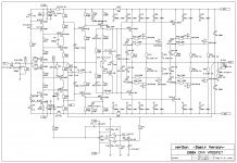 200W CFA 1.3.2-sch.jpg401.6 KB · Views: 994
 -
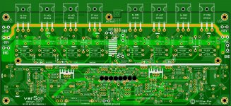 200W CFA 1.3.2b photo.jpg473.5 KB · Views: 991
 -
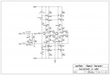 balanced in add-sch 1.2.jpg157.2 KB · Views: 973
 -
 balanced in board.jpg201.1 KB · Views: 942
 -
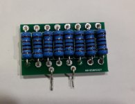 FB board.jpg275.9 KB · Views: 881
 -
 PS regulator oard 2.jpg390.9 KB · Views: 354
 -
 PS regulator board 1.jpg339 KB · Views: 396
 -
 PS regulator-mosfet-duallayer-sch1.2.jpg313 KB · Views: 421
Damir:
PM sent.
sorry for the delay!
mlloyd1
PM sent.
sorry for the delay!
mlloyd1
Now I have all boards here, but I am missing the PayPal email address from:
tjencks
mlloyd1
please send PM with PayPal address and I'll send the money request.
Damir
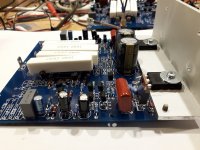
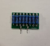
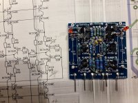
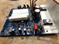
There two types of small boards to be soldered on to main power board.
1. CFA Feedback board for unbalanced version, contains 8 1k1 2W 1% metal film resistors, first photo. Two pins to solder on to main power board.
2. Balanced add board with balanced inputs, soldered instead first one. In this case no need for CFA FB board from first photo. Six pins to solder on to main power board.
BR Damir
Attachments
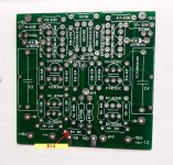
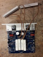
There was a question about some soldering of the 200W CFA board.
There are two way to use this amp, with unbalanced input and balanced inputs.
1. For unbalanced input there is small additional board with Feed Back resistors. It should be soldered to the main board via holes FB and MID (blue arows) marked on the schematic and the main board.
It is showed on first three pictures. Bear in attention to solder that small board as the last soldering as it can be on the way to older small components on the main board on the proximity of it.
2. Similar way is for small balanced in board, but there more connections, +-15V, +in, –in, gnd and of course FB and MID.
It is showed in fourth and father on picture. This small board could disturb main board soldering, so again solder it as the last.
Important think no to forget, check that P1 is set to max value before connect the power and start to adjust the bias current.
Best regards Damir
Attachments
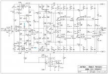
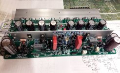

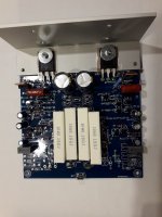
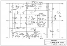
This MOSFET PS regulator contains following protection: overcurrent protection, loudspeaker DC offset protection and protection against bigger then allowed differences in +- output voltage. If any protection was triggered both power supply polarity will switch off simultaneously. To switch on again it is necessary to switch off the mains power for few minutes to allow big caps to discharge.
All component can be assembled for first power on, minus switcher transistors Q7 and Q107. This is because minus output polarity should be set equal positive output polarity first. Put some load on both outputs, I use 2 x 330R 10W resitors between out +- and ground.
If there is output voltage on the out + - and it should be 6 to 7 volts lower then in + - .
When that was set solder in transistors Q7 and Q107. Now is possible to test the PS regulator. With 0.075R for R9 and R109(This will limit to about 20 A, to lover it short one diode D3 and D103) the current sensing transistors Q6 or Q106 should trigger Q8, Q9 or Q108, Q109. Those transistors are in the configuration similar to thyristor and when triggered transistor Q7 or Q107 will conduct and switch of output serial transistor Q13, Q113.
The pins LL and LR are DC offset sensor inputs when connected to the power output. Connect there 10 V or more (to any input) and it will trigger the same “thyristors” with delay defined with RC constant of R18/C4, R19/C5 (similar on minus side) and switch off the outputs transistors.
One important feature is instantaneous switch off of both polarity because of differences in the output voltage recognized via zeners D6 and D7.
This board could be used for stereo amp, than need to be solder both DC sensors, and if used as dual mono then use only one.
Damir
PS. The photos show PS regulator version for three channel amp, only difference is more connections and three DC sensing inputs instead of two.
Attachments

Last edited:
Here is my DIY packaging of your great SOTA power amplifier design. We had trouble finding blue LED source with consistent and even light output. Think they nailed it now.
Two, two-channel amps are needed for Bi-Amp'ed JBL M2 system.

Chassis is all CNC milled parts.... top, bottom, front, back.
THx-RNMarsh
Two, two-channel amps are needed for Bi-Amp'ed JBL M2 system.
Chassis is all CNC milled parts.... top, bottom, front, back.
THx-RNMarsh
Last edited:
- Home
- Amplifiers
- Solid State
- 200W MOSFET CFA amp