I've been looking at many a pcb layout these days. One thing that many comments stress is that the typical big "U" made for the ground all around the board is a bad thing, as it creates a big loop around the small signal section.
Question being, would the following approach, making a smaller "U" in the middle of the board, in between the input and output sections be any better or are there pitfalls in there too ?
Subsidiary question: can I cross over the bottom of the U with the output resistors, in order to bring the output node close to the input and make a short feedback path or should I lay those horizontal and bring the feedback network over the ground ?
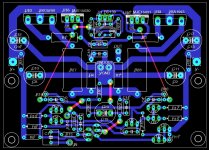
An exemple of what I mean is attached (it is a symasym, standard names for it, see Mike's website)
Question being, would the following approach, making a smaller "U" in the middle of the board, in between the input and output sections be any better or are there pitfalls in there too ?
Subsidiary question: can I cross over the bottom of the U with the output resistors, in order to bring the output node close to the input and make a short feedback path or should I lay those horizontal and bring the feedback network over the ground ?
An exemple of what I mean is attached (it is a symasym, standard names for it, see Mike's website)
Attachments
I'll admit to doing the U style layout myself and have spent some time this year trying to revise some layouts to get away from this. I started with something similar to what you have done, it is an improvement as it pretty much halves the effective track length.
I do wonder if it really makes much difference though for class-b power amps, the issue is loop areas and it tends to be switching or sharp edged signals that have EMC problems.
I do wonder if it really makes much difference though for class-b power amps, the issue is loop areas and it tends to be switching or sharp edged signals that have EMC problems.
Well actually it does have some effect which obviously will be noticeable with highly sophisticated equipment .
The size of the problem will be equal to the sensitivity that the ""traces"" of your drivers might have under specific conditions .
On real life and under extensive tests ( and since many of the amplifiers we work with will not worth investigation and/or production of highly sophisticated 2 layer pcbs ) i noticed that if you are about to hardwire something to avoid the U issue and in general ""all around ground "" situations it will be better to hardwire ground IE:
brake it in two areas ground +small signal ground hardwire one with the other down under the board and reverse decoupling to be relocated in the inner area of the pcb and in a central position related to ground .
Similar to that you may feature power supply caps on board opposite side of output transistors keep small signals close to PSU ( minimizes needs on decoupling ) and hardwire flying leads to power the transistors only +local decoupling with return to ground again in the center of the board to preserve a star ground as much is possible
Both solutions worked very well for the P3A amplifier who happens to be even more sensitive in terms of decoupling .
Both solutions looks far more safe than flying leads on the drivers which is a more case sensitive section .
Kind regards
Sakis
Keep your input ground separate! Cover the whole top of the board with ground plane, but have a separate one for input section.
Two-sided pcbs are easy to make at home.
No way GOTEE this is not of any use in audio amplifiers ....
which part are you disagreeing with?No way GOTEE this is not of any use in audio amplifiers ....
Keep Signal Ground separate from Power Ground
or
Cover the top of the PCB with a Ground Plane
or
Have a separate section for Signal (Ground)
or
Two-sided PCBs are easy to make at home
I am inclined to agree.
I keep seeing from the RF experts the recommendation to "always" use planes even in noraml audio circuits.
I keep thinking "why".
What does a plane bring to an audio amplifier?
Each time I see that I think again hoping to see the light but never come to blankly accept the recommendation.
Just yesterday, I saw and thought again !!!
The HF/RF takes the least impedance route. That Return Route follows the Signal Route on the adjacent plane. (they don't suggest a plane for the Signal they still do that by defined traces.
But, at lower frequencies the Return does not necessarily follow the signal trace. At very low frequencies, i.e. audio, the Return takes the lowest resistance route across the plane. That lowest resistance route is likely to be the SHORTEST point to point length across the PCB. That route may now include a "loop" ready to become an interference receiver for other low frequency fields, eg. hum and it's low harmonics. HF interference will still look at the HF Return route as lowest impedance and thus see near zero loop area with shunting capacitance to attenuate voltage differentials.
Another thought:
Could the Shortest Return Routes become "shared" routes with other point to point currents? Would this create interference voltages?
Keep your input ground separate! Cover the whole top of the board with ground plane, but have a separate one for input section.
Agreed

And power rails + power GND close together. The loop continues all the way to the power supply. All sensitive small signal circuitry outside of high current loop(s).
A good way is to picture the current from transformer to speaker and back. What loops are present and what circuits are inside the loops?
This was the Dr Cherry recommendation from a couple of decades ago.
Yes. It makes sense and is actually quite easy to layout especially for a symmetrical amp.
My take on ground planes is that they can be of benefit but you need to know what you are doing. I don't so stay well clear.
I am inclined to agree.
I keep seeing from the RF experts the recommendation to "always" use planes even in noraml audio circuits.
I keep thinking "why".
What does a plane bring to an audio amplifier?
Each time I see that I think again hoping to see the light but never come to blankly accept the recommendation.
Just yesterday, I saw and thought again !!!
The HF/RF takes the least impedance route. That Return Route follows the Signal Route on the adjacent plane. (they don't suggest a plane for the Signal they still do that by defined traces.
But, at lower frequencies the Return does not necessarily follow the signal trace. At very low frequencies, i.e. audio, the Return takes the lowest resistance route across the plane. That lowest resistance route is likely to be the SHORTEST point to point length across the PCB. That route may now include a "loop" ready to become an interference receiver for other low frequency fields, eg. hum and it's low harmonics. HF interference will still look at the HF Return route as lowest impedance and thus see near zero loop area with shunting capacitance to attenuate voltage differentials.
Another thought:
Could the Shortest Return Routes become "shared" routes with other point to point currents? Would this create interference voltages?
Ground plane is NOT mainly for RF benefits or reasons!
The best reason for the plane, I think, is to keep all of the loop areas as small as possible. Otherwise, you make hum antennas, as well as RF antennas.
The next-best reason is probably to mitigate the sharing of ground conductor by different currents. Significant voltages are induced across inductance (and resistance) of the shared ground conductors, themselves. Do you want those voltages to be arithmetically summed with the input to your high-gain power amplfier?!
It is entirely appropriate for audio, which is almost always sub-optimal without it (although how audible that might be can vary widely).
It's probably the easiest way for someone inexperienced at layout to get a fairly-good result, "first time, every time".
It is so easy to do that there is basically no good-enough excuse for not doing it. Why do people resist?
AndrewT, by the way, current does not take the path of least impedance. Current takes ALL paths, in inverse proportion to their impedances. [It is easy to construct an example where almost all of the current flows in paths other than the lowest-impedance one. (Hint: You just need a large number of the higher-impedance paths.)]
Cheers,
Tom
This is where you lose me. If a current takes all paths then does this not make loop area an unknown quantity?
I don't know if its significant but doesn't a ground plane create a small capacitance with every track?
It is so easy to do that there is basically no good-enough excuse for not doing it. Why do people resist?
Conversely - its so easy to do that people do it without thinking if its actually optimal for audio. Its not, I know because I've listened. I do not resist ground planes I merely do not go there. The reason being common ground impedance coupling - no planes have zero impedance and you don't want your noisy power ground to couple into your signal.
Therefore two ground planes, one for signal ground and one for power ground could be OK, provided they connect together only at a single point. But having two planes on your board either means you have to go more than two layers (practically impossible to DIY) or there's simply nowhere for any other tracks to be placed.
With two ground planes (signal, ground) the problem comes at inputs and outputs, which typically have common-mode ground currents flowing in them. You most certainly do not want to contaminate your signal ground with them, but power ground is too noisy....... Any ideas?
I found the most important things is star grounding to one point.
I built a USB controlled mixer and just connected up the pcb any which was easiest.
The result was loads of noise which ruined the project. Extra decoupling and more earthing wires didn't help.
I tracked down the noise to charging impulses into the smoothing capacitors.
So I redesigned the pcb keeping the smoothing capacitors on separate ground lines and it worked a treat with very little noise.
Any grounds that have charging impulses or high currents should be starred.
Conversely - its so easy to do that people do it without thinking if its actually optimal for audio. Its not, I know because I've listened. I do not resist ground planes I merely do not go there. The reason being common ground impedance coupling - no planes have zero impedance and you don't want your noisy power ground to couple into your signal.
Therefore two ground planes, one for signal ground and one for power ground could be OK, provided they connect together only at a single point. But having two planes on your board either means you have to go more than two layers (practically impossible to DIY) or there's simply nowhere for any other tracks to be placed.
With two ground planes (signal, ground) the problem comes at inputs and outputs, which typically have common-mode ground currents flowing in them. You most certainly do not want to contaminate your signal ground with them, but power ground is too noisy....... Any ideas?
It's simple: Just use separate sections of non-overlapping ground planes, all on the component side of the board.
I would have a separate one for the signal input section's ground, for sure. I mentioned that in my previous post, by the way.
The rest is mostly power ground.
The idea is that a plane should have much lower impedance than any single trace. But, of course, if the currents happened to all tend to clump into one path on the plane, because of the layout, then regular traces with star grounding might be almost as good, in that case, at least in terms of the reason for star grounding.
For anything for which you would normally have a separate ground leaving the board, use a separate section of ground plane, or just use traces if it makes more sense (i.e. only one or two ground connections for that type of ground). (But then you probably wouldn't get the benefit of optimally-small loop areas. So use the plane.)
If you try a ground plane, you will love how easy it makes the layout.
ALTERNATIVELY, envision using traces but always keeping the return or ground for each one directly opposite from it, on the other side of the board from it, exactly overlapping. That gives minimum loop areas! e.g. For every power trace and signal trace, imagine running an identically-shaped ground trace on the other side of the board from it. (But when there are series components in a trace, then a ground plane will generally be significantly better at keeping the loop area small, and with much less layout effort.)
I would keep the two power traces together, for example, and run ground opposite them, always overlapping them, on the other side of the board.
But, if you grasp the reasons for that, then you might also see that it's a lot easier (and also electrically better) to just flood the one whole side with ground, then (or, rather, most likely with several separate areas of different types of grounds).
And yes, mcd99uk, there will be a small capacitance formed between the ground plane on one side and the power traces (et al) on the other side. That's a nice bonus! If you can use 1mm or thinner pcb stock, the capacitance can be significant-enough to be helpful at very high frequencies. It's like having evenly-distributed HF decoupling caps, everywhere.
ALSO, a good layout will be MUCH easier to achieve, because almost all of the ground traces will be out of the way, on the other side of the board (in the form of ground planes). (Imagine how much easier it would be if we could also move all of the power traces to other planes!)
The only additional pain that I foresee is that when doing two-sided PCBs at home, we don't usually have plated-through holes. So you have to manually solder wires into any via holes, or solder leads on both sides of the board, if you want a trace to connect on both sides.
The biggest pain is components like large radial electrolytics, and things like terminal blocks, where it's basically impossible to solder them on the component side of the board. For those, you just need to makes traces on both the top and bottom that go just outside of the component's perimeter and place a via pad on both sides, there, and solder a short piece of wire through the hole, on both sides (assuming it's something that needs to also connect on the top side ground plane, which will usually be the case for electrolytics, although they will typically have one pin that ONLY connects to the top, and not the bottom, which is done very similarly, i.e. only on one side of the board instead of both, at the "outer" end of the short "via trace").
Cheers,
Tom
Last edited:
")
This is where you lose me. If a current takes all paths then does this not make loop area an unknown quantity?
I don't know if its significant but doesn't a ground plane create a small capacitance with every track?
That part about the current taking all paths wasn't really part of my point. Sorry. It's just that it's so rare for me to see a chance to "correct" anything that AndrewT says that I couldn't help myself. <grin!>
Using a ground plane should still minimize all of the enclosed loop areas on the PCB, with the least layout design effort and the greatest effectiveness, while also offering a lower-impedance ground path to minimize the voltage noise created by currents sharing the same conductor.
But we still would want a short and fat (low inductance and resistance) path from any plane to the star ground, and separate paths to the star ground for any grounds that need to be quiet (input) and for any that have very large or dynamic currents (output?).
Last edited:
- Status
- This old topic is closed. If you want to reopen this topic, contact a moderator using the "Report Post" button.
- Home
- Amplifiers
- Solid State
- amplifier PCB, question on overall grounding layout