.... for these Greg designed the GB100 - although I don't think it ever came to market.
Bigun, Greg does sell the GB100D, but I don't know if that's what you meant...
Member
Joined 2009
Paid Member
I don't bother with calculations much these days, I let LTSpice do them for meHow do you predict by calculation the voltage ...

Anyhow it appears that I need to eliminate the emitter degeneration to get the max tempco if I want to use the QFETs. Plus, neither option detracts much from the pcb layout as I can use the same pads to install a resistor, a link or a diode wired transistor like Greg's baseline design and do the experiments later if warranted.
Stuey - you're right, I wasn't paying attention !
It's not the frequency that's the problem with mosfets. A square wave at half rail amplitude is worst case power dissipation in the output devices
Along with ~2/3 sine wave. With a large square wave signal, the high rate of change can create a small amount of cross conduction during each zero crossing in some output stages designed for AF. Increasing frequency increases the overall cross conduction and then 'Poooffff!' --


Even for analog operation, I'm a fan of using totem pole drive for each gate.
This along with local dampening components is a small price to pay to be able to very accurately control the mosfet. Square wave tests can point out certain instabilities. It is possible that an amp may be fairly stable with 100nf load but will oscillate with 10nf. Square wave test can easily find such an issue. Perhaps of lesser importance, a fast square wave can show slew limitation. Building amps at home and for learning, I have formed an opinion that it is good to slightly over design for and press the output stage a bit further in testing than you would expect normal operation. It gives a cushion of limitation. That being said, if you can achieve stable bias, I would experiment with how much power these mosfets can really take. They are cheap and a few are expendable for testing. I blistered my finger on the plastic package once in such a test Dohh!
 and it didn’t fail for nearly another minute! Then as expected the N-ch failed.
Member
Joined 2009
Paid Member
The current source also controls the turn-on of the amp. The RCR mod shown in post 18 slows down the turn on because the capacitor has to charge via the resistors before the current source becomes active. I believe Greg went so far as to use very high resistor values (I saw 470k quoted somewhere). The slower turn on reduces the current surge through the output MOSFETs. This is not only safer but also helps minimize any turn-on noises at the output.
I believe the value of the capacitor is important though - too large and it can create problems still because of different turn on rates of the top/bottom halves of the amp which produces a turn-on thump. A 10uF cap seems to work well in simulations and is also the value Greg uses in the RCR mod from what I have read so far. The MOSFET source resistors are also going to limit the turn on surge to some extent.
I plan to start on the pcb layout soon. I'm tempted to try something new and different from Greg's but on the other hand it seems silly to reinvent what is proven to work well.
Cross-conduction - I don't know much about this. I figure it's mostly a failure of a device to switch off. In this amplifier the FET gates are actively pulled off by the driver devices. The drivers have a lower output impedance when switching the output FETs off than they do when turning them on. I figure this is a good thing and that a totem pole drive is not necessary ?
Last edited:
I don't bother with calculations much these days, I let LTSpice do them for me
Anyhow it appears that I need to eliminate the emitter degeneration to get the max tempco if I want to use the QFETs. Plus, neither option detracts much from the pcb layout as I can use the same pads to install a resistor, a link or a diode wired transistor like Greg's baseline design and do the experiments later if warranted.
Stuey - you're right, I wasn't paying attention !
Hi Bigun
Can you change the ratio of the 3k resistor and the one in the current source to increase the compensations for the QFets?
Fab
......................... Increasing frequency increases the overall cross conduction ...................
I always recommend Input filtering that defines the passband of the Power Amplifier.GB bandwidth limited the input anyway, so cross conduction should be avoided.................
Sensible RF filtering will limit the rise time of any input signal.
Member
Joined 2009
Paid Member
Can you change the ratio of the 3k resistor and the one in the current source to increase the compensations for the QFets?
I would have to play with the Sims again, but what I saw is that the ratio of resistors in the current source allow tempco to be tuned. The other resistor is the MOSFET source resistor.
I am thinking about generating the bias on one rail only and mirroring to the other. This neatly ensures both LTPs start up together
I believe the current sources are not the only factor on start up - the non-complimentary turn-on characteristics of the output FETs is also significant.
Member
Joined 2009
Paid Member
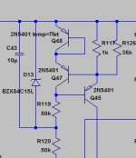
So I have looked into the 'zener mod' that is written about and made my best guess. See first attachment. The zener diode pins the voltage at the junction of the two resistors of the current source tail to a fixed drop from the power rail. This acts like a 'super diode', a shunt regulator that works all the way down to d.c. In my sims is offers nearly a 10x improvement in PSRR at d.c. over a small capacitor by itself. It looks like a good tweak and I understand it has been popular.
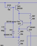
I'm leaning towards a slightly different solution, an emitter follower regulated current source. See second attachment. I've added a simple emitter follower to the power rail feeding the current source. A zener diode fixes the voltage so it will act like a voltage regulator. In simulations at least, it is vastly superior to the 'zener mod' described above in terms of stabilizing the d.c. performance of the amplifier since it essentially regulates the front end.
It also provides a very controlled and slow turn-on for the current source because it also behaves like a 'capacitance multiplier' of JLH fame. This allows the in-rush current to the MOSFETs to be strictly limited.
It also provides a good deal of PSRR improvement - this is probably as good as it gets for the current source PSRR for simple arrangements. The PSRR of the amplifier is mostly dominated by the current source but once the PSRR of the current source is reduced to these levels then there are more subtle factors in the inter-play between the amplifier stages - possibly a diminishing returns scenario.
The tempco of my emitter follower buffered current source is unaffected by this change and in the form shown it's simulating at around 16mV/degC (not sure that this is sufficient for the QFET as yet though).
Attachments


Member
Joined 2009
Paid Member
Of course, it's gonna kill the CFB-SKA hybrid, but you knew that already
No, seriously, I want to produce something close to the original. But it won't be exactly the same - mostly because it makes no sense to clone Greg's amp when you can buy it from him for such a good price - it'd never be worth the time and effort.
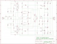
So I want to add my own 'stamp' to the design. This will be limited to a couple of simple tweaks. First, the current source mod to include the RCR in the source tail, second to add the cap-multiplier and third I'm eliminating the diode-wired transistor. And I feel this is in the spirit of things since Greg does advocate tweaking the current source in his baseline design.
I am also going to include a provision for resistors in the 'unused' collectors of the LTPs - a 'trick' from a forum member called 'SandyK' so that the Early effect is more balanced.
I am using separate source resistors for the output devices to encourage current sharing (when two devices are used).
That's about it. I've attached an updated schematic from Eagle (hint: open the image in a new tab in your browser as it will then allow you to magnify it further, making it much easier to read).
In updating the schematic I realized I'm not interested in reproducing Greg's pcb design. Mostly because it's stupid - just go and buy one from him. But also because I want to take advantage of parts I can get in SMD format. I've replaced all the small signal devices with surface mount parts in SOT-23-6 packages. These are not that small, in fact a lot easier than the SOT-363 I used on TGM5. In this package you can get pnp-npn pairs which I need 3 per amplifier, and dual matched pairs of pnp and npn for the LTP. The manufacturer matches the die far more closely than I could - simply because it's difficult to measure things that accurately without creating controlled conditions for the measurements and buying lots of parts to sort from.
I also want to use connectors for the signal input, for the power supply and speaker output, rather than soldering in fly-wires to the board. I used connectors on my first 3 amplifiers and found them nice to have.
No, seriously, I want to produce something close to the original. But it won't be exactly the same - mostly because it makes no sense to clone Greg's amp when you can buy it from him for such a good price - it'd never be worth the time and effort.
So I want to add my own 'stamp' to the design. This will be limited to a couple of simple tweaks. First, the current source mod to include the RCR in the source tail, second to add the cap-multiplier and third I'm eliminating the diode-wired transistor. And I feel this is in the spirit of things since Greg does advocate tweaking the current source in his baseline design.
I am also going to include a provision for resistors in the 'unused' collectors of the LTPs - a 'trick' from a forum member called 'SandyK' so that the Early effect is more balanced.
I am using separate source resistors for the output devices to encourage current sharing (when two devices are used).
That's about it. I've attached an updated schematic from Eagle (hint: open the image in a new tab in your browser as it will then allow you to magnify it further, making it much easier to read).
In updating the schematic I realized I'm not interested in reproducing Greg's pcb design. Mostly because it's stupid - just go and buy one from him. But also because I want to take advantage of parts I can get in SMD format. I've replaced all the small signal devices with surface mount parts in SOT-23-6 packages. These are not that small, in fact a lot easier than the SOT-363 I used on TGM5. In this package you can get pnp-npn pairs which I need 3 per amplifier, and dual matched pairs of pnp and npn for the LTP. The manufacturer matches the die far more closely than I could - simply because it's difficult to measure things that accurately without creating controlled conditions for the measurements and buying lots of parts to sort from.
I also want to use connectors for the signal input, for the power supply and speaker output, rather than soldering in fly-wires to the board. I used connectors on my first 3 amplifiers and found them nice to have.
Attachments
Last edited:
Member
Joined 2009
Paid Member
Hi Paulo,
Well... progress has beena bit slow on account of the day-job (business travel) but I have been looking at parts choices and thinking about the mechanical layout.
I'm comfortable that I can get good quality semi-conductors in SMT and I've chosen the following parts from Digikey for all the small signal transistors:
For the LTP: DMM5401 and DMM5551 matched paris, with 2% matching on Hfe, Vce and Vbe. The packaging can handle the power dissipation just fine and being SOT-23-6 sized packages they are DIY friendly.
For the current source/sink and driver devices: I selected PBSS4160DPN which gives me npn-pnp pairs. They are not matched for parameters but their temperatures will track nicely. These are in a SOT457 package, which for all intents and purposes is the same as the SOT-23-6. They are low Vce sat which is handy for the drivers.
I'm not happy with SMD devices for electrolytic capacitors, things may have improved over the past couple of years but I don't think they are as good as through-hole. They are also less DIY friendly because their contacts are not easy to solder by hand despite being large. I have chosen to use through-hole capacitors instead.
Resistors will be mostly 1206 size as I find this a good DIY-friendly size. I know many DIYers use smaller but I like 1206. I've used them before, they're big enough to run traces under if you have to (done that on single sided boards) and the printed values are readable - they allow me to use higher wattage parts which I feel leads to better performance.
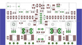
For the mechanical layout I prefer to avoid pcb stand-offs, it always seems to be a challenge getting all the holes to line up and installing them neatly. I prefer to bolt through the pcb and power devices in one-go. For my TGM1 amplifier I used a flanged heatsink style but for TGM5 I held the pcb flat on top of the power devices. It worked well, it's stable and easy to build. However, the pcb gets heated by the devices. For this project, TGM7, I will bolt the pcb over the power devices but use the temperature sensing TO-126 packaged devices inbetween the power device and pcb to provide a gap. This has the benefit of putting the temperature sensing device in intimate contact with the power devices to reduce the impact of the heatsink heat-capacity slowing down the thermal feedback loop.
I've put together a 'first draft' mechanical layout which I'm not yet satisfied with; some parts may be moved to the underside, no point wasting real-estate. As this will be my first commercially made pcb I figure I'll take full advantage of it being double-sided. I like to keep high current circuits all at one side of the board.
Well... progress has beena bit slow on account of the day-job (business travel) but I have been looking at parts choices and thinking about the mechanical layout.
I'm comfortable that I can get good quality semi-conductors in SMT and I've chosen the following parts from Digikey for all the small signal transistors:
For the LTP: DMM5401 and DMM5551 matched paris, with 2% matching on Hfe, Vce and Vbe. The packaging can handle the power dissipation just fine and being SOT-23-6 sized packages they are DIY friendly.
For the current source/sink and driver devices: I selected PBSS4160DPN which gives me npn-pnp pairs. They are not matched for parameters but their temperatures will track nicely. These are in a SOT457 package, which for all intents and purposes is the same as the SOT-23-6. They are low Vce sat which is handy for the drivers.
I'm not happy with SMD devices for electrolytic capacitors, things may have improved over the past couple of years but I don't think they are as good as through-hole. They are also less DIY friendly because their contacts are not easy to solder by hand despite being large. I have chosen to use through-hole capacitors instead.
Resistors will be mostly 1206 size as I find this a good DIY-friendly size. I know many DIYers use smaller but I like 1206. I've used them before, they're big enough to run traces under if you have to (done that on single sided boards) and the printed values are readable - they allow me to use higher wattage parts which I feel leads to better performance.
For the mechanical layout I prefer to avoid pcb stand-offs, it always seems to be a challenge getting all the holes to line up and installing them neatly. I prefer to bolt through the pcb and power devices in one-go. For my TGM1 amplifier I used a flanged heatsink style but for TGM5 I held the pcb flat on top of the power devices. It worked well, it's stable and easy to build. However, the pcb gets heated by the devices. For this project, TGM7, I will bolt the pcb over the power devices but use the temperature sensing TO-126 packaged devices inbetween the power device and pcb to provide a gap. This has the benefit of putting the temperature sensing device in intimate contact with the power devices to reduce the impact of the heatsink heat-capacity slowing down the thermal feedback loop.
I've put together a 'first draft' mechanical layout which I'm not yet satisfied with; some parts may be moved to the underside, no point wasting real-estate. As this will be my first commercially made pcb I figure I'll take full advantage of it being double-sided. I like to keep high current circuits all at one side of the board.
Attachments
Last edited:

Member
Joined 2009
Paid Member
I didn't realize there was a difference - do you mean that 15mm fuses are rare and not available ?
I suppose we can always order them from the States but the standard here is 20mm. I've never used a 15mm fuse, the ones I buy everywhere are 20mm.
Member
Joined 2009
Paid Member
I see. Well I will look at fitting in 20mm - although I'm not sure that my pcb is going to be 'good enough' for wider use yet.
I am nervous about routing of the gate connections.
It looks to me as if there's no clean way to keep the gate wiring away from the heavy current traces of the output/power rails when using two pairs of outputs. The gate traces will either pass near-by or cross over/under on opposite side of the board some of these high current paths.
Since the gate drive is low impedance (from the emitters of the drivers) and there will be gate-stoppers at the gate pins I am thinking it maybe safe because capacitive coupling will be swamped out and hence negligible compared with the internal parasitic capacitances of the FETs themselves. I'm probably worrying without good reason. Opinions would be welcome ??
I see. Well I will look at fitting in 20mm - although I'm not sure that my pcb is going to be 'good enough' for wider use yet.
I am nervous about routing of the gate connections.
It looks to me as if there's no clean way to keep the gate wiring away from the heavy current traces of the output/power rails when using two pairs of outputs. The gate traces will either pass near-by or cross over/under on opposite side of the board some of these high current paths.
Since the gate drive is low impedance (from the emitters of the drivers) and there will be gate-stoppers at the gate pins I am thinking it maybe safe because capacitive coupling will be swamped out and hence negligible compared with the internal parasitic capacitances of the FETs themselves. I'm probably worrying without good reason. Opinions would be welcome ??
Use the gate stoppers as bridges, even if the lead spacing needs to be wider than normal, to cross the D/S traces at 90deg. R to G trace minimised, of course!
I didn't realize there was a difference - do you mean that 15mm fuses are rare and not available ?
Certainly common ones here are M205 (20mm) and 3AG which are even bigger.
If the gate stopper pad is right next to the gate lead then only a short length of resistor lead + trace length + FET lead add a little inductance "after" the stopper.
For those that want even lower inductance. Don't use this pad. Attach the stopper resistor directly to the FET gate lead right where it comes out of the package. The closer the resistor body is to the gate lead the better.
Other traces can now pass under that resistor VERY close to the gate lead and no interference due to low capacitive coupling to the now raised resistor body.
- Home
- Amplifiers
- Solid State
- TGM7 - an amplifier based on Greg Ball SKA