You could try posting your proposed schematic. Not many here will have
used rare parts like those museum pieces or any other Vfet in class A.
Perhaps this would be would be a way to encourage people to think about it.
The rail voltages suggest this is not intended for class A but are other designs
on the site close to what you are considering?
AMPLIMOS one stage amplifiers, amplificatori audio monostadio
These FETs needs some heavy offset voltage on the gate to conduct.
The MONSTRE probaply won't do this without modification, but the circuit that Ian posted ( Hiraga 30W Class A) would probably work.
So maybe if you add the two 8.2K resistors to the gate in the Monstre it would become possible.
Please recalcuate the value of the resistors though.
The MONSTRE probaply won't do this without modification, but the circuit that Ian posted ( Hiraga 30W Class A) would probably work.
So maybe if you add the two 8.2K resistors to the gate in the Monstre it would become possible.
Please recalcuate the value of the resistors though.
Last edited:
It could be... however the link that Ian put has some other circuits you might wanna explore before deciding to experiment with Hiragas.
Like this!
Anyway if you are going for the Hiraga please notice that the N-channel 2SK82 needs some 10-12V negative voltage on the gate, and the 2SJ28 needs the same ballpark figure positive voltage on the gate!!!
The circuit is somewhat self-balancing since the outputs are in the feedback-loop of the drivers/VAS individually, but start slowly on a variotrafo or with fuse/reistors in series with the supply. Then measure that the outputs are conducting and that the circuit is performing well before going on full power.
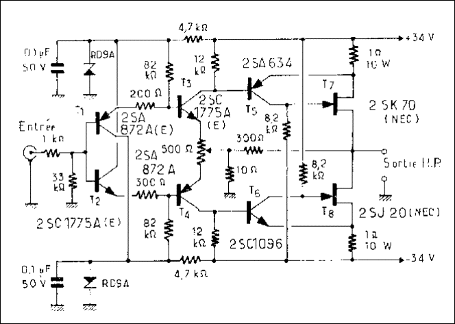
With all due respect to Mr. Hiraga, the proposed schematic shows he did not tryly understand how a SIT/VFET works, which is even more surprising considering he was profficient in designing tube (specifically triode) circuits.
DO NOT attempt that schematic as it will not work correctly.
One important thing the schematic is not showing you is that the source terminals of the SIT/VFET are at the output of the amp. Contrary to what Nrik says these parts do NOT need voltages on the agte to conduct, these are depletion mode and with no voltage on the gate (Vgs=0V) will conduct heavily. What they do need is a negative voltage at the gate to STOP them from conducting. The actual voltage that drives then into cut-off deneds on Vds - one more thing where they differ from any other kind of FET. These parts are for all intents and purposes a solid-state triode, and as such ALL of the terminals are inputs. The current Id depends on both Vgs and Vds, with a ratio of mu, a quantity known from triodes as the amplification factor. For 2SK80/2SJ28 this is about 10 on the average (varies with chosen operating point, they are extremely linear at Vds much higher than in the schematic). And this brings us to the problems with the schematic itself.
Mr Hiraga rather unwisely simply transposed his 'darlingnot' circuit which is current driven, into an attempt to make the current of the BJT driver stage into driving voltage for the SIT/VFETs. There are several problems with this:
1) A relatively minor problem is that the required bias voltage for a chosen bias current depends on the power supply voltage. In other words, any sag or ripple will modulate the bias current. The only logical solution that would keep the schematic simple, would be to regulate the power supply.
2) A much bigger problem is what actual bias current the amp will have. There is no means to change it in this simple circuit, and this us really a big problem because the SIT/VFETs have very high tolerances. The 2SK82/2SJ28 available on eBay from acronmanelectronics are actually quite good with this since they all belong to the same 'rank' - VFETs were originally sorted into 'ranks', corresponding to a cut-off voltage. When paralleling or using complements, the idea was to use the same rank in order to get the same characteristics. Acronman sells the same rank for both the P and N part - the rank code is the last digit of the datecode (typically KD33), rank 3. The rank is loosely defined as the Vgs at which Id=100mA at Vds=50V. The encoding is (7.5 + R*2.5)V, where R is the rank number, except for ranks 0 and 1.
Still, this leaves you with the need to adjust various part values in the schematic to get the required bias current. And, with a different pair, it might differ as much as 30% even with the same rank number on the VFETs.
3) MUCH bigger problem, a fundamental one, is a gross mistake in the setup of the circuit which will result in it's destruction when full output is attempted, either voltage or current. Here is why:
If you look at the driver arrangement, the collectors of the driver BJTs are returned to the oposite power supply so that the circuit can give negative gate voltages with respect to the output, where the sources are. But what happens when the output gets close to one of the power supplies? Say, the +V power supply? Well, to do this, the gate of the top VFET is driven more positive, but the gate of the bottom VFET gets less and less 'negative' (with respect to it's polarity) gate drive because there is less and less available negative voltage on the bottom 8.2k resistor. So instead of the top VFET conducting more, and the bottom less, in order to drive the output towards the top rail, the bottom VFET actually starts at some point when the output is approaching the supply rail, to conduct more and more, so current is passed from the + to the - supply. In order for the output to get closer to the rail it requires even more drive which makes the situation even worse, until the circuit latches up. If the heat has not killed it, something else will and that is driving Vgs positive without current limit.
In any case when very high output current is needed, the driver will attempt to connect G to D via it's C-E region. This will drive Vgs positive, into gate current. The problem here is that there is no current limit to the gate drive. The VFET is actually capable of operating in 'enhancement mode' which is actually more like a regular BJT - it exhibits beta (current amplification Ids/Igs, roughly 50 for this type), but the G-S region is a diode and it's absolute maximum current is about 0.5A. For a short circuit on the output (or very low impedance) only the 1 ohm resistor provides a current limit and this may still pass an excessive current through G-S. It will certainly happen in a latch-up condition as mentioned above.
Finally, VFETs are VERY fast. Especially the K82/J28. These were originally used in a class D output stage switching at 0.5MHz, a figure which manufacturers achieve today only within the confines of a single chip, and even then it's a rarity. In the original amplifier that used these parts, the DISCRETE design was able to achieve switching times of about 50nS which is equivalent to output slew rate of 4kV/us. YES they can and often will oscillate without a gate stopper. Add one, it will also limit the gate current.
How to fix this?
1) Regulate the power supply, or provide a means for bias voltage to track the power supply (this would however severely reduce the PSRR figure of the amp so regulation would be a better idea).
2) Provide a means of adjusting the bias voltages. This is not as simple as it requires simultaneous adjustment of two resistors, or an adjustmet of the resistance of a center-tapped balance pot. Also, getting exactly complementary K82/J28 is not easy unless you are willing to do matching amongst a larger contingent. To make things worse, static (DC) and dynamic (AC) balance is not the same thing. A dynamic balance scheme could be incorporated into the schematic, along with the static one already present.
3) Provide floating or bootstrapped power supplies fot he gate drive. Bootstrapping is a must but even in that case having the output stuck close to the rail longer than the bootstrap constant will kill the output stage. Added positive and negative supplies at 2x main supply (aasy to do with voltage doublers and simple regulation) is the right way to go. Provide a means of switching off the main power supply when these are not present (easy to do by providing the reference voltage for the main PSU regulation from these auxilliary power supplies).
4) Add some gate stopper resistors to the gates of the K82/J28. While at it, the 8.2k resistors are really on the high side for driving the input capacitance of the original VFETs specified in the schematic (nearly 1.5nF for the J20! about half that on the K70). K82/J28 are very low capacitance but it's still not trivial. More current through the driver transistors can help.
...and don't try to save money on the heatsink. VFETs are actually extremely robust parts but overheating will kill them. On the plus side, no need to worry about thermal stability, they have negative tempco and in fact for currents over 0.5A it's almost zero.
Thanks to Ilimnz for the proper description.
To toot my horn I will say that my point was the same regarding bias, Ilimnz just described it more precise.
And regarding ripple the original Hiraga circuit with bipolars definitely also needed supply regulation or CRC network, so that is not just down to the V-FET parts. Probably everybody who has build this circuit or Le Monstre ( which was meant to run on batteries) can confirm this.
hi all
I think the schematics on the amplimos site would be very good ,he certainly seems to know his stuff when it comes to these devices
I will send him a pm and see what he recommends ,who knows maybe we could organise to get some boards made ,with his permission of course
the devices are pricey but readily availiable from acronman and well worth the effort from what nelson and mr amplimos says
Sheafer
Most of these schematics disregard the problem of bias current dependency on power supply voltage / ripple. The result is intermodulation with the ripple in the PSU. Ordinairly in a tube PP amp the output is transformer coupled and fed from the same power supply do the ripple largely cancels out, and the bias dependency is far lower because the gm of tubes is a small fraction of that of VFETs. A look at various schematics of amps that used VFETs in their original era, shows a few tricks to circumvent this problem, and in fact every VFET amp has some form of compensation for this - even the Yamaha B1 which has regulated main power supplies. Ditto the problem of bias voltage availability - even though its often done with power sequencing relying on certain values of filter caps in the PSU to insure the bias voltage come sup before the main voltage (and I can tell you from experience it's not a fool-proof method!).
Use of VFETs to their full ability is not a simple as one might think...
Use of VFETs to their full ability is not a simple as one might think...
Ilimzn how is this different from other traditional emitterfollowers with bipolar or MOSFETs?Most of these schematics disregard the problem of bias current dependency on power supply voltage / ripple. The result is intermodulation with the ripple in the PSU.
please explain.
...so what you are saying is that the bias voltage should be present BEFORE the supply voltage on the V-FETs (?) ...that makes sense since 0V bias at start-up would mean FULLY OPEN V-FETsDitto the problem of bias voltage availability - even though its often done with power sequencing relying on certain values of filter caps in the PSU to insure the bias voltage come sup before the main voltage (and I can tell you from experience it's not a fool-proof method!).
Use of VFETs to their full ability is not a simple as one might think...

Very important - thank you for highlighting this.
- Status
- This old topic is closed. If you want to reopen this topic, contact a moderator using the "Report Post" button.
- Home
- Amplifiers
- Solid State
- lemonstre with 2sk82/2sj28