Hi Andrew,
Sorry, I was messy.
R4 belongs to the Sx amp schematic, it's 15 ohms. That one is removed, but still on the BOM "description" row.
C4-C5 and C7-C8 belong to the PSU, and can be seen on the PCB drawing on your PDF and on the PCB itself.
As you say these caps are no longer fitted, the only abnormality I found up to now is R4 on the amp BOM. The item qty as been reduced from 8 to 7, but not the description)
Maybe the best solution to avoid mistakes would be to list all the changes from the v1.0 PCB on the thread first post ?
Sorry for the unclear messages...
There are no high gain, high Vceo, cbe transistors in that list !
Nor any ebc.
did you read post1727?Think it has to do with Bonsais comercial products")
Yes of course.
To be clear:
https://www.ovationhifidelity.com/products/
To be clear:
Thank you!
Class A Model 1727 will come later in 2017!
https://www.ovationhifidelity.com/products/
Thats F5V2 pcb from cvillers. Bonsai have a very good and easy to follow schema for "Zero Noise". I have asked Bonsai if this way of connecting two output pcb to one transformer can be "transformed" to the F5V2( the pcb have originally no decoupling condensers)
Eivind S
Eivind S
Bonsai, you have PM
But my photos , you will find in this post.
Eivind Stillingen
Eivind,
From what I can see, I don't think your proposal is going to work like that.
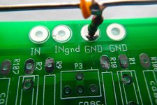
You need to lift the signal ground i.e. INgnd via a 15-22 ohm resistor in order to break any ground loops.
Its important also to know whether or not the INgnd has only signal return connections on the PCB. If not, you could have problems.
Can you post up the schematic for your amplifier?
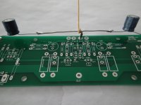
Ingnd and out GND share the same pad and are directly connected. I was "afraid" that this is the reason why your very clear schema how to connect two amplifires pcb does not fit in with the way cvillers pcb is lay out.
It is this kind of drawing that you have brought I need. Not long threads and many post with mixed use of ground in, ground out, zero(0) etc. And also an endless discussion that confuses more than clear things up.
Schema:
http://www.diyaudio.com/forums/pass-labs/254056-f5turbo-illustrated-build-guide.html
Eivind S
F5 Post1 sch.
I think there is a misprint. Why is R25 different value from R26?
Edit. That is confirmed in the text.
The four capacitors C1, 2, 5 & 6 come together to form the decoupling ground. This then becomes the Power Ground. If you are building a monoblock, then this can also be the Main Audio Ground from which all other voltage references can be taken.
R2 and R3/4 are Signal Return. These need a voltage reference to the Main Audio Ground. This voltage reference passes nearly zero current and passes interference current. A bit of resistance in this near zero current link does no harm.
But it is worth checking that there is no DC current flowing along this link. A DC voltage error here will increase the output offset.
If you add some resistance between Signal Return and Main Audio Ground, then you must also add in a mains fault current route to bypass that added resistance. This bypass takes fault current appearing on the input sockets to chassis and thence to PE. It would be this route that would blow the fuse in a faulty source component that does not have a working PE.
I think there is a misprint. Why is R25 different value from R26?
Edit. That is confirmed in the text.
There is one error in this schematic - R26 should be 10K
The four capacitors C1, 2, 5 & 6 come together to form the decoupling ground. This then becomes the Power Ground. If you are building a monoblock, then this can also be the Main Audio Ground from which all other voltage references can be taken.
R2 and R3/4 are Signal Return. These need a voltage reference to the Main Audio Ground. This voltage reference passes nearly zero current and passes interference current. A bit of resistance in this near zero current link does no harm.
But it is worth checking that there is no DC current flowing along this link. A DC voltage error here will increase the output offset.
If you add some resistance between Signal Return and Main Audio Ground, then you must also add in a mains fault current route to bypass that added resistance. This bypass takes fault current appearing on the input sockets to chassis and thence to PE. It would be this route that would blow the fuse in a faulty source component that does not have a working PE.
Last edited:
Here is the link showing how to wire your amp boards up to the main power supply. Note carefully how the wires are twisted and also how to 'T' off the filter capacitor 0V connection to avoid hum. Note, you may not need the ground lifter (that is the bottom bridge rectifier shown on page 2). I would build your amp without it - only install the ground lifter if you really need it.
For the speaker return wiring, I have shown it on page 2 going directly back to the 'T'. You will get an improvement if you take this back to the amplifier 0V from the speaker return socket and you also twist it with the speaker + output wire. Keep the loop areas small where possible - twisting is a good way to do this.
The diagram on page 2 shows separate rectifiers for each secondary. The scheme still works if you use a single bridge rectifier to simulateously generate the + and - supply voltages
http://hifisonix.com/wordpress/wp-c.../How-to-wire-up-a-Power-Amplifier_Updated.pdf
Here is how you need to connect the input to your amp boards, and how to connect the additional decoupling capacitors:-
Attachments
Last edited:
I have reached the wiring stage for the Sx.
Fig 21 on the pdf shows at least 11 wires connected to the terminal block. I don't quite explain them all. here are the ones I foresee :
- mains earth : 1
- speakers gnd : 2
- transformer screen : 1
- PSU gnd lift J3 : 1
- the amp boards GND seem to come straight from the PSU board, so not through the GND terminal block.
Well, it seems on Fig 20 that no GND lifter is used on this amp. But it does not explain the 6 missing wires... What did Ioverlook ?
Additionally, if the inputs are grounded with the J2 jumper, what's the use of the SIG 0V terminals on the PSU pcb ?
Other question : in the Sx pdf PSU test instructions page 40 :
"making sure the main rectifier is coupled with heatsink grease to the base of the chassis"
Is this still applicable ? I don't see how with the present Sx PSU pcb...
- Home
- Amplifiers
- Solid State
- SX-Amp and NX-Amp