Hi guzz,
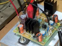
I Like Your Idea to fasten contact bricks on the toroidal transformer via wooden plate!
It looks not vey nice, but it is very practical !")
Agreed! this is DIY so do what you like so long as it will not hurt you or others.
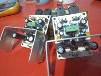
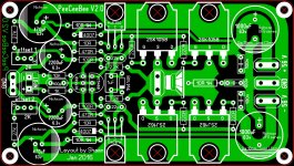
that is nice compact layout
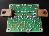
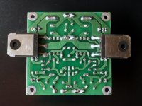
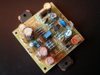
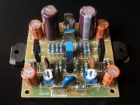
final update :
- C3503 & A1831
- Pan FC
- mix Takman & Dale resistors
noticable better instruments position

Attachments


Hello Fellow DIYers! 
Here goes the PDFs for the PeeCeeBee V3!!
Wishing you all a Merry Christmas and Happy New Year!!!
shaan
Here goes the PDFs for the PeeCeeBee V3!!
Wishing you all a Merry Christmas and Happy New Year!!!
shaan
Attachments
-
V3 Overlap.pdf27.3 KB · Views: 496
-
V3 Mask.pdf9 KB · Views: 427
-
V3 Silkscreen.pdf14.6 KB · Views: 485
-
V3 Layout.pdf13.8 KB · Views: 631
-
 DSC05359.JPG796.6 KB · Views: 560
 -
 DSC05360.JPG615.8 KB · Views: 724
 -
 DSC05364.JPG792 KB · Views: 1,753
 -
 DSC05356.JPG712.2 KB · Views: 1,969
 -
 v3 Xray.jpg109.4 KB · Views: 1,997
 -
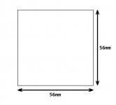 V3 Dimensions.jpg20.6 KB · Views: 1,905
Hi Shaan
I see the feedback electrolytics in the power GND now!
Since February 2016!
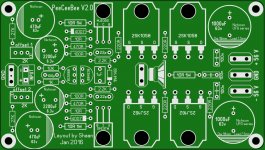
Hello Shaan
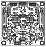
I retouched Peeceebee V2.0 pcb.
I will use Nichicon UFG series Audio Grade Electrolytic Capacitors
Nichicon UFG series capacitors diameter is bigger than other capacitors.
Gerber and lay files attached
I retouched Peeceebee V2.0 pcb.
I will use Nichicon UFG series Audio Grade Electrolytic Capacitors
Nichicon UFG series capacitors diameter is bigger than other capacitors.
Gerber and lay files attached
Attachments

New Shaan designed pcb is with feadback caps on power gnd,please make the same on your's.Hello Shaan
I retouched Peeceebee V2.0 pcb.
I will use Nichicon UFG series Audio Grade Electrolytic Capacitors
Nichicon UFG series capacitors diameter is bigger than other capacitors.
Gerber and lay files attached
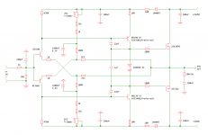
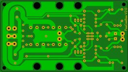
The reason the feedback caps in V3 were routed to the power ground is quite obvious as soon as we see the board layout, to accommodate all the components on that tiny board. V2 is more spacious compared to V3 so this trick is unnecessary. Also in V2 the nearest ground traces to the feedback section is too long to ensure a clean feedback ground. Notice that the feedback caps in the V3 is directly connected to the power GND with small dedicated traces, which I think is not possible in V2 just because of the size of the board.
Ok i got it!The reason the feedback caps in V3 were routed to the power ground is quite obvious as soon as we see the board layout, to accommodate all the components on that tiny board. V2 is more spacious compared to V3 so this trick is unnecessary. Also in V2 the nearest ground traces to the feedback section is too long to ensure a clean feedback ground. Notice that the feedback caps in the V3 is directly connected to the power GND with small dedicated traces, which I think is not possible in V2 just because of the size of the board.
hay shaan, i have a few question
- Can i, add 3 more pair output stage & how many watt if use 4 pair ouput stage?
- In schematic V3 (post #2187) how to setting & measurement 2 pcs trimer for maximum amp performance?
Thank's, gyw
Hi gyw.
- Adding more pairs won't give you more power in the same load unless you increase the PS voltage as well. You can add 4 pairs and with +/-70V and get maybe 500W into 4R load (you will need to add/remove a lot of other stuffs for the amp to work well at that voltage). Even if you don't increase voltage but instead decrease load impedance for more power, emitter followers between the VAS and OPS will be necessaary for any VAS load above 2nF. Bottomline - not recommended in the default PeeCeeBee config.
- In V3 the trimmers are there mainly to zero the offset. Initially VAS bias is auto-set to between 5mA and 15mA by the 15K resistors. The trimmers will help to some extent to increase/decrease a VAS bias that is too low or too high. 10mA is a good VAS bias in V3 for overall good performance (100mV around VAS emitter resistors). OPS bias is auto-set by 1N4148 diodes. As preferred in the BOM and schema, using MJE340G/350G or any other high gain pair for the VAS instead of BD pair will increase performance.
- Home
- Amplifiers
- Solid State
- PeeCeeBee