My friend recently gave me this botched up amplifier. It supposedly was a DIY job, from some kit. Apparently one channel worked, the other didn't. In any case, I just dismantled the entire thing because the MDF enclosure that it was in had mould growing all over it after being left in the corner of a workshop for 10 years and the wiring was horrid. And apart from the transformer, nothing in the case was even screwed in place.
The only discerning labels on the board are "RIM electronic" and "NFK 50". The company apparently exists (existed?) but I can't find anything about this model. I assume the 50 means 50 watts which seems to be about right for the output transistors: a 2n3055 and a BDX18, both in TO-3 cases mounted onto their own heatsinks.
Here the circuitboard, the output transistors (along with the driver transistors) are mounted on the heatsinks.
I found the reason for one channel not working, the base pin of the driver transistor of the PNP output transistor has been pulled off the package. That and a burnt out resistor (I'm guessing a couple of things near by went poof as well).
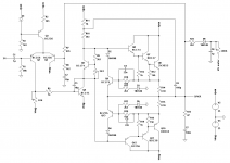
Yesterday and today, in the process of figuring out which terminals goes to what I managed to reverse engineer a schematic. Please excuse my messy drawing
So now I ask you, does this look ok? I'm not really knowledgable about linear analog circuits other than basic opamps and such. And I still have to check the part values. There are three trimpots in there for adjusting things (bias I assume, the third one is to adjust the scale on the analog VU meter), how would I go about checking that they're set right?
I still have to check the health of power transformer (which also appears to be a DIY job and by it's weight I'd call it slight overkill). In the enclosure I found some scribbles suggesting "23V" for the power supply, I'm guessing thats bipolar (the wiring is so bad that that I can't even tell). The power supply was built on turret board and was just a basic bridge rectifier and two 4700uF 50V capacitors but I'm going to rebuild the entire thing anyway.
The only discerning labels on the board are "RIM electronic" and "NFK 50". The company apparently exists (existed?) but I can't find anything about this model. I assume the 50 means 50 watts which seems to be about right for the output transistors: a 2n3055 and a BDX18, both in TO-3 cases mounted onto their own heatsinks.
Here the circuitboard, the output transistors (along with the driver transistors) are mounted on the heatsinks.
An externally hosted image should be here but it was not working when we last tested it.
I found the reason for one channel not working, the base pin of the driver transistor of the PNP output transistor has been pulled off the package. That and a burnt out resistor (I'm guessing a couple of things near by went poof as well).
Yesterday and today, in the process of figuring out which terminals goes to what I managed to reverse engineer a schematic. Please excuse my messy drawing
An externally hosted image should be here but it was not working when we last tested it.
An externally hosted image should be here but it was not working when we last tested it.
So now I ask you, does this look ok? I'm not really knowledgable about linear analog circuits other than basic opamps and such. And I still have to check the part values. There are three trimpots in there for adjusting things (bias I assume, the third one is to adjust the scale on the analog VU meter), how would I go about checking that they're set right?
I still have to check the health of power transformer (which also appears to be a DIY job and by it's weight I'd call it slight overkill). In the enclosure I found some scribbles suggesting "23V" for the power supply, I'm guessing thats bipolar (the wiring is so bad that that I can't even tell). The power supply was built on turret board and was just a basic bridge rectifier and two 4700uF 50V capacitors but I'm going to rebuild the entire thing anyway.
Alright, spotted a section of the schematic I missed, checked all the part values and redrew it in LTSpice (where the circuit functions so I guess I got right!).
On one channel the BD138 PNP transistor mounted on the heatsink next to the lower output transistor is destroyed, the base pin is ripped out of the package. The 150ohm resistor with the capacitor parallel to it at the base of Q13 has some charring on it but measures correctly. Other components around there measure strange but most components do when they're in a circuit . The closest thing for a replacement to that transitor that I've found in my drawers is a TIP32C, would that function or should I order something closer? Other than that I've got a bunch of TO220 package transistors. I'm not going for pristine sound here, just the learning experience and satisfaction of fixing stuff.
So along with fixing that issue, I still need some guidelines on how to approach adjusting the trimmers when I get it fixed, I just need to know what to look for (I've got a scope)
On one channel the BD138 PNP transistor mounted on the heatsink next to the lower output transistor is destroyed, the base pin is ripped out of the package. The 150ohm resistor with the capacitor parallel to it at the base of Q13 has some charring on it but measures correctly. Other components around there measure strange but most components do when they're in a circuit
. The closest thing for a replacement to that transitor that I've found in my drawers is a TIP32C, would that function or should I order something closer? Other than that I've got a bunch of TO220 package transistors. I'm not going for pristine sound here, just the learning experience and satisfaction of fixing stuff.So along with fixing that issue, I still need some guidelines on how to approach adjusting the trimmers when I get it fixed, I just need to know what to look for (I've got a scope)
Attachments
It's a standard "Lin" topology amplifier using a Triple Darlington output stage. I'd say it's probably from the very late 1970s - early 1980s judging by the transistors.
If you've got a dead Q11, then it's possible the output Q10 is damaged. A TIP32C should function. BD137/BD138 were popular driver transistors at the time. Remember that TO-220 pinout is backward from TO-126. If you lost Q10 then an MJ2955 would now be the transistor of choice.
The transistors being on separate heatsinks could be a problem. Is D2 or Q5 mounted on the heatsink?
Modern BD139/140 devices are substandard compared to the Philips devices that will have been prevalent when this amplifier was made. TIP32C will function, it just will not be optimal. Though, if you want to get "optimal" the answer will be to scrap the circuit and build something similar with modern parts.
Wow, thanks for the great replies
Here is a photo the transistor mounted on the heatsink (the TO3 package is visible on the other side, the 150ohm resistor soldered directly between the emitter and base with the driver transistor screwed on nearby). This is NPN side, the other side is identical, the circuitboard is sandwiched between the two heatsinks with standoffs.
Apart from Q7 and Q8, Q10 and Q11 and a top hat heatsink on Q4 nothing is heatsinked-
Among other visible casualites, along with the Q11 and R20, I also noticed that Q12 has disintegrated (one pin completely disconnected from the cracked pacakge) and Q5 is chipped away on the side as well if the sheds any light on the subject. The junction between the base and collector seems to be shorted.
Among resistors that have iffy values are R13 and R19 (around 200ohms instead of 1k), R10 (700ohms inteas of 3k3), R11 (also around 700 instead of 1k). I'm getting conductivity over C6 too. I wrongly read the colour bands, R16 and R20 are actually 180ohms, the burnt R20 measures 140ohms.
And if I measure from the positive to the negative power rail it shows 370ohms.
On the other channel of the amp all these components measure what they visually indicate with any abnormalities. So it looks like the output transistors are shot too.
I'll try and get the other channel working before I tackle this. The amount of things that need to be replaced are making the "optimal" choice rather appealing If nothing else I got 9 pounds of transformer out of this
Here is a photo the transistor mounted on the heatsink (the TO3 package is visible on the other side, the 150ohm resistor soldered directly between the emitter and base with the driver transistor screwed on nearby). This is NPN side, the other side is identical, the circuitboard is sandwiched between the two heatsinks with standoffs.
Apart from Q7 and Q8, Q10 and Q11 and a top hat heatsink on Q4 nothing is heatsinked-
An externally hosted image should be here but it was not working when we last tested it.
Among other visible casualites, along with the Q11 and R20, I also noticed that Q12 has disintegrated (one pin completely disconnected from the cracked pacakge) and Q5 is chipped away on the side as well if the sheds any light on the subject. The junction between the base and collector seems to be shorted.
Among resistors that have iffy values are R13 and R19 (around 200ohms instead of 1k), R10 (700ohms inteas of 3k3), R11 (also around 700 instead of 1k). I'm getting conductivity over C6 too. I wrongly read the colour bands, R16 and R20 are actually 180ohms, the burnt R20 measures 140ohms.
And if I measure from the positive to the negative power rail it shows 370ohms.
On the other channel of the amp all these components measure what they visually indicate with any abnormalities. So it looks like the output transistors are shot too.
I'll try and get the other channel working before I tackle this. The amount of things that need to be replaced are making the "optimal" choice rather appealing
If nothing else I got 9 pounds of transformer out of this Not really relevant, but I came across something quite similar to this a while back. Thought I'd share.
See here: http://www.diyaudio.com/forums/soli...mono-amplifiers-2sk135-2sj50-little-help.html
See here: http://www.diyaudio.com/forums/soli...mono-amplifiers-2sk135-2sj50-little-help.html
The power supply is +-30V (2x22V on the transformer).
I got the other channel working and properly set the bias and offset, gpt a complete set of voltage measurements ands hooked up a speaker to listen to some tunes. It does 57 volts peak to peak without clipping.
The heatsinks are about 9x9cm with 12 fins protuding out 2.5 cm.
I've just desoldering a bunch of components from the broken channel and so far the death toll is every transistor from Q4 onwards except the BDX18 and the BD137 and the diode D4 . I'm going to rig up a better test the multimeter's diode test to check those two that survived.
I got the other channel working and properly set the bias and offset, gpt a complete set of voltage measurements ands hooked up a speaker to listen to some tunes
. It does 57 volts peak to peak without clipping.The heatsinks are about 9x9cm with 12 fins protuding out 2.5 cm.
I've just desoldering a bunch of components from the broken channel and so far the death toll is every transistor from Q4 onwards except the BDX18 and the BD137 and the diode D4
. I'm going to rig up a better test the multimeter's diode test to check those two that survived.Well I might as well finish this story... it now works!
I wasted two hours yesterday wondering why it was giving me -18V on the output until I finally realised I put a PNP transistor in for Q4 instead of an NPN . I replaced all the smaller transistors with MPSA06/MPSA56, the driver transistors for BD139/BD140 and just replaced the dead NPN output transistor with another 2n3055 that I already had. That and a diode and one of the 2watt resistors.
I also changed the R2 resistor from 3k3 to 2k2 because the offset adjust didn't get low enough (and if its designed to be adjustable it should adjust to 0)
Here is one channel hooked up on my temporary test jig:
The transformer shows it's age but it functions. The power supply only has 2x4700uF, I'll probably redo it with some bigger caps and proper fuses and such.
Now to just get an enclosure for this thing and turn it into a useable piece of equipment
Thanks for the help guys!
I wasted two hours yesterday wondering why it was giving me -18V on the output until I finally realised I put a PNP transistor in for Q4 instead of an NPN
. I replaced all the smaller transistors with MPSA06/MPSA56, the driver transistors for BD139/BD140 and just replaced the dead NPN output transistor with another 2n3055 that I already had. That and a diode and one of the 2watt resistors.I also changed the R2 resistor from 3k3 to 2k2 because the offset adjust didn't get low enough (and if its designed to be adjustable it should adjust to 0)
Here is one channel hooked up on my temporary test jig:
An externally hosted image should be here but it was not working when we last tested it.
The transformer shows it's age but it functions. The power supply only has 2x4700uF, I'll probably redo it with some bigger caps and proper fuses and such.
Now to just get an enclosure for this thing and turn it into a useable piece of equipment
Thanks for the help guys!
- Status
- This old topic is closed. If you want to reopen this topic, contact a moderator using the "Report Post" button.
- Home
- Amplifiers
- Solid State
- Fixing up/reverse engineering this old amp (2n3055+BDX18)