trouble shooting HB update.
Thank you for the response, I should have the Transistor tester today, when that arrives I will re check each transistor if good I will put them back in. Can I leave the power transistor's out until I test under power if that checks out then put the power transistors back in?
I read somewhere on here there is an option to do that but for the life of me I can't find it. that process was using some resistors in place of the Power transistor's?
You can run it without the output transistors installed but you need to connect the feedback circuit. To do this you would connect a resistor between base and emitter pad on one positive rail output resistor and one negative rail output resistor. 1k should work there. Another option is to install one pair of output transistors.
DC offset troubleshooting.
I will give that a try to see if all is well with the world, I should be able to see no dc voltage on the DC offset between Ouput and Ground? Correct.
You can run it without the output transistors installed but you need to connect the feedback circuit. To do this you would connect a resistor between base and emitter pad on one positive rail output resistor and one negative rail output resistor. 1k should work there. Another option is to install one pair of output transistors.
I will give that a try to see if all is well with the world, I should be able to see no dc voltage on the DC offset between Ouput and Ground? Correct.
No avail still a issue
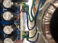
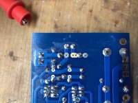
Good morning, I checked all the transistors out of the circuit they all passed with the diode check on the MM and the Peak Atlas DCA. I double check each component again in the circuit all are good, check for shorts from the heat sink to the transistors all is good. No shorts I can find anywhere.
I put two 1K resistors across the base and Emitter on One positive power transistor instead of the power transistor, and One on the negative side.
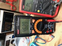
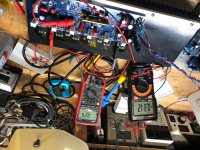
powered it up with a bulb tester and variac with 20 volts + and - and measured from the Output to the Ground and the DC voltage climbed to 4. volts, I removed the 1K load resistors and no DC voltage across the Output to Ground.
I am wondering if I am getting power from the PSU on the ground side, I Show 0v across the ground of the board on the input from the two rectifiers, and when I measure the voltage from V+ to Ground I get 63+ and V- to Ground I get -63V.
The rectifiers are wired to the same transformer with two secondary's,
Where do I go from here?
You can run it without the output transistors installed but you need to connect the feedback circuit. To do this you would connect a resistor between base and emitter pad on one positive rail output resistor and one negative rail output resistor. 1k should work there. Another option is to install one pair of output transistors.
Good morning, I checked all the transistors out of the circuit they all passed with the diode check on the MM and the Peak Atlas DCA. I double check each component again in the circuit all are good, check for shorts from the heat sink to the transistors all is good. No shorts I can find anywhere.
I put two 1K resistors across the base and Emitter on One positive power transistor instead of the power transistor, and One on the negative side.
powered it up with a bulb tester and variac with 20 volts + and - and measured from the Output to the Ground and the DC voltage climbed to 4. volts, I removed the 1K load resistors and no DC voltage across the Output to Ground.
I am wondering if I am getting power from the PSU on the ground side, I Show 0v across the ground of the board on the input from the two rectifiers, and when I measure the voltage from V+ to Ground I get 63+ and V- to Ground I get -63V.
The rectifiers are wired to the same transformer with two secondary's,
Where do I go from here?
Attachments
It sounds like your input stage isn't working correctly. Start by measuring the voltage drop across R20 and R21. They should both be pretty close to the same. Figure out the current flows through the current mirrors from that (divide the voltage reading by the resistance). It should be around 1.5mA each.

No voltage drop
R20 and R21 are both correct values of 220 R I have not applied full power to the circuit as of yet, around 20 volts applied I get voltage to ground on both sides of the R20 and R21 around -14 volts and across R20 drop of .0150 and .0093 on R21.
I received new BC550C for Q1 and Q2 Replaced the Mpsa18, the pinouts are reverse of the Mpsa18 Made sure I had them in correctly. they are the reverse orientation which does not allow zip tie to tie them. on the collector of each of those I see 10V on the emiter I see only-.9 on one and - 1.4 on the other
I have to agree with you something is not correct in the input but for the life of me I cannot figure what it is. this should have been paint by numbers with the parts in the correct orientation and location. I have my doubts that these new boards 2.4 are correct although that doesn't make sense.
It sounds like your input stage isn't working correctly. Start by measuring the voltage drop across R20 and R21. They should both be pretty close to the same. Figure out the current flows through the current mirrors from that (divide the voltage reading by the resistance). It should be around 1.5mA each.
R20 and R21 are both correct values of 220 R I have not applied full power to the circuit as of yet, around 20 volts applied I get voltage to ground on both sides of the R20 and R21 around -14 volts and across R20 drop of .0150 and .0093 on R21.
I received new BC550C for Q1 and Q2 Replaced the Mpsa18, the pinouts are reverse of the Mpsa18 Made sure I had them in correctly. they are the reverse orientation which does not allow zip tie to tie them. on the collector of each of those I see 10V on the emiter I see only-.9 on one and - 1.4 on the other
I have to agree with you something is not correct in the input but for the life of me I cannot figure what it is. this should have been paint by numbers with the parts in the correct orientation and location. I have my doubts that these new boards 2.4 are correct although that doesn't make sense.
Still burning
Not using the Variac, just bulb limiter, the R25 resistor went up in smoke with in 1 min. 60+ 0 -60 on the power in. Across R20 and R21 no measurable voltage. in the .0012 range DC. Voltage across the GRD and Output over 40 volts.
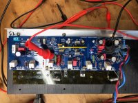
I did trace with a MM the connections from q1 q2 q3,4 q5,6 all are good solid connections reflowed many of the solder joints to make sure I had good solid connections. here is what I am using for Transistor's. I did replace MPSA18 with BC550CTA but that did not change the outcome.
Q1 NPN Input Transistor (LTP) 610-MPSA18
Q2 NPN Input Transistor (LTP) 610-MPSA18
Q3 NPN Transistor (Cascode/Current Mirror) KSC1845 512-KSC1845FTA
Q4 NPN Transistor (Cascode/Current Mirror) KSC1845 512-KSC1845FTA
Q5 PNP Transistor (Cascode/Current Mirror) KSA992 512-KSA992FBU
Q6 PNP Transistor (Cascode/Current Mirror) KSA992 512-KSA992FBU
Q7 NPN Transistor (LTP CCS) KSC1845 512-KSC1845FTA
Q8 NPN Transistor (LTP CCS) KSC1845 512-KSC1845FTA
Q9 PNP Transistor (VAS/CCS) KSA992 512-KSA992FBU
Q10 PNP Transistor (VAS/CCS) 2SA1381 KSA1381ESTU
Q11 NPN Transistor (VAS/CCS) 2SC3503 512-KSC3503DSTU
Q12 NPN Transistor (VAS/CCS) 2SC3503 512-KSC3503DSTU
Q13 NPN Transistor (VBE Multiplier) 2SC3503 512-KSC3503DSTU
Q14 NPN Driver Transistor MJE15032 863-MJE15032G
Q15 PNP Driver Transistor MJE15033 863-MJE15033G
Q16 NPN Output Transistor NJW0281 863-NJW0281G
Q17 NPN Output Transistor NJW0281 863-NJW0281G
Q18 NPN Output Transistor NJW0281 863-NJW0281G
Q19 PNP Output Transistor NJW0302 863-NJW0302G
Q20 PNP Output Transistor NJW0302 863-NJW0302G
Q21 PNP Output Transistor NJW0302 863-NJW0302G
Your input stage isn't running. Try losing the Variac and just running the bulb limiter. The voltage drop on R20 and R21 should be around 0.3V.
Not using the Variac, just bulb limiter, the R25 resistor went up in smoke with in 1 min. 60+ 0 -60 on the power in. Across R20 and R21 no measurable voltage. in the .0012 range DC. Voltage across the GRD and Output over 40 volts.
I did trace with a MM the connections from q1 q2 q3,4 q5,6 all are good solid connections reflowed many of the solder joints to make sure I had good solid connections. here is what I am using for Transistor's. I did replace MPSA18 with BC550CTA but that did not change the outcome.
Q1 NPN Input Transistor (LTP) 610-MPSA18
Q2 NPN Input Transistor (LTP) 610-MPSA18
Q3 NPN Transistor (Cascode/Current Mirror) KSC1845 512-KSC1845FTA
Q4 NPN Transistor (Cascode/Current Mirror) KSC1845 512-KSC1845FTA
Q5 PNP Transistor (Cascode/Current Mirror) KSA992 512-KSA992FBU
Q6 PNP Transistor (Cascode/Current Mirror) KSA992 512-KSA992FBU
Q7 NPN Transistor (LTP CCS) KSC1845 512-KSC1845FTA
Q8 NPN Transistor (LTP CCS) KSC1845 512-KSC1845FTA
Q9 PNP Transistor (VAS/CCS) KSA992 512-KSA992FBU
Q10 PNP Transistor (VAS/CCS) 2SA1381 KSA1381ESTU
Q11 NPN Transistor (VAS/CCS) 2SC3503 512-KSC3503DSTU
Q12 NPN Transistor (VAS/CCS) 2SC3503 512-KSC3503DSTU
Q13 NPN Transistor (VBE Multiplier) 2SC3503 512-KSC3503DSTU
Q14 NPN Driver Transistor MJE15032 863-MJE15032G
Q15 PNP Driver Transistor MJE15033 863-MJE15033G
Q16 NPN Output Transistor NJW0281 863-NJW0281G
Q17 NPN Output Transistor NJW0281 863-NJW0281G
Q18 NPN Output Transistor NJW0281 863-NJW0281G
Q19 PNP Output Transistor NJW0302 863-NJW0302G
Q20 PNP Output Transistor NJW0302 863-NJW0302G
Q21 PNP Output Transistor NJW0302 863-NJW0302G
If higher supply voltage doesn't improve anything the next step would be to measure base to emitter voltage on the transistors in circuit. There needs to be around .6V difference between the two to turn the transistor on. If you are seeing less than that you need to investigate why there's no difference. If you are seeing substantially higher than that there is usually an issue with the transistor you are measuring.
HB troubleshooting at a standsill.
Indeed I have done that I have even removed the trimmers and double checked that.
I traced the connections and all seam to be in order, I checked and rechecked the values of the components all are in order, I have double checked all the values of the caps the one cap that is bi Polar is correct all others are installed correctly.
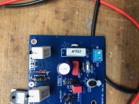
R25 goes up in smoke as soon as I apply full power, I replace the transistors Q1 and Q2, with very close matches and insured there installed correctly.
I am stumped, I have built 3 Wammys, 5 Chip amps, 2 waynes line Stages, and never had this type of problem.
I hate to do it but a might just disassemble the board piece by piece and start over, that will not tell me what the heck is wrong.
All suggestions are greatly appreciated.
I have to ask. Did you set R17 (1Kohm pot) to 500ohm before you installed it?
And R7 around 85ohm.
Indeed I have done that I have even removed the trimmers and double checked that.
I traced the connections and all seam to be in order, I checked and rechecked the values of the components all are in order, I have double checked all the values of the caps the one cap that is bi Polar is correct all others are installed correctly.
R25 goes up in smoke as soon as I apply full power, I replace the transistors Q1 and Q2, with very close matches and insured there installed correctly.
I am stumped, I have built 3 Wammys, 5 Chip amps, 2 waynes line Stages, and never had this type of problem.
I hate to do it but a might just disassemble the board piece by piece and start over, that will not tell me what the heck is wrong.
All suggestions are greatly appreciated.
"I hate to do it but a might just disassemble the board piece by piece and start over, that will not tell me what the heck is wrong."
I would probably have done one board myself already. Do one board at a time then you may find your mistake on the other board. Possibility problem with boards but doubtful. Crap does happen sometime.
I would probably have done one board myself already. Do one board at a time then you may find your mistake on the other board. Possibility problem with boards but doubtful. Crap does happen sometime.
Thank you for pointing that out.
Yes sir good catch, I did fix that and it has not improved the issue.
I just spotted one mistake. C1. You must solder one leg closest to the input connector. And then you need to solder in the link next to C1.
Yes sir good catch, I did fix that and it has not improved the issue.
Attachments
No need to strip the boards. You just need to narrow down where your problems are coming from. R25 is burning up so Q9 is passing too much current. For this to happen the base voltage of Q9 must be too low. This would be happening because the input stage isn't running. While sorting this out, leave R25 off the board and figure out why the input stage isn't running.
If you can measure base to emitter voltage and mark them on on a schematic and post a picture of the schematic it helps others figure out where your issues lie. Also mark voltage drops on input stage resistors.
If you can measure base to emitter voltage and mark them on on a schematic and post a picture of the schematic it helps others figure out where your issues lie. Also mark voltage drops on input stage resistors.
No need to strip the boards. You just need to narrow down where your problems are coming from. R25 is burning up so Q9 is passing too much current. For this to happen the base voltage of Q9 must be too low. This would be happening because the input stage isn't running. While sorting this out, leave R25 off the board and figure out why the input stage isn't running.
If you can measure base to emitter voltage and mark them on on a schematic and post a picture of the schematic it helps others figure out where your issues lie. Also mark voltage drops on input stage resistors.
Thank you I will check into that tomorrow and report back.
Good news today
I got the one board up and running, Finally, here is what I found.
the old schematic and BOM that is on the Store is just that; old. I am not 100% sure that is what caused all the issues but I am sure that both boards did the same thing and anything I tried until I change these items would Not work. Might be because of the Parts are newer and some specs changed from when the old BOMwas published. Really don't know.
"mbrennwa" published a new BOM and Schematic Jan 2017 for version 2.4 and it has several different values for resistors in R3 R6 R23 R24 R26 and capacitor change c5 to 100uf as well. I replaced those items recheck all the work put the old transistor's back in except q1 and q2 changed them out to MPSA06. I also changed out D1 D2 to 1N914 the old BOM said you could use 4148.
Crossed my fingers and pressed the power button and I got low DC offset, .3 v and a Bias at .25mv
I haven't run a signal through it yet but will today, now I have to redo the second board to get it to work with the same changes. that will be interesting, stay tuned will keep you all posted if I get this up totally.
Thank you I will check into that tomorrow and report back.
I got the one board up and running, Finally, here is what I found.
the old schematic and BOM that is on the Store is just that; old. I am not 100% sure that is what caused all the issues but I am sure that both boards did the same thing and anything I tried until I change these items would Not work. Might be because of the Parts are newer and some specs changed from when the old BOMwas published. Really don't know.
"mbrennwa" published a new BOM and Schematic Jan 2017 for version 2.4 and it has several different values for resistors in R3 R6 R23 R24 R26 and capacitor change c5 to 100uf as well. I replaced those items recheck all the work put the old transistor's back in except q1 and q2 changed them out to MPSA06. I also changed out D1 D2 to 1N914 the old BOM said you could use 4148.
Crossed my fingers and pressed the power button and I got low DC offset, .3 v and a Bias at .25mv
I haven't run a signal through it yet but will today, now I have to redo the second board to get it to work with the same changes. that will be interesting, stay tuned will keep you all posted if I get this up totally.
Attachments
the new boards and old BOM/schematic can not be the root of the problem. I've build a 5ch amp last year with the 2.4 boards, and used the BOM from the store. Unliky you, i used SS9014 for Q1,Q2. And VAS/VBE transistors are not the same. Othervise it's all the same. And i hadd no isues with the amp. It has been running for a year now with no problems what so ever. Wel, there is one difference. I don't use the LC cap.
- Home
- Amplifiers
- Solid State
- diyAB Amp The "Honey Badger" build thread