Looking for a little help on a DX Blame build, it’s the supercharged version.
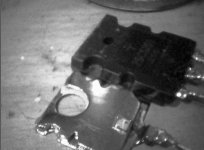
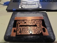
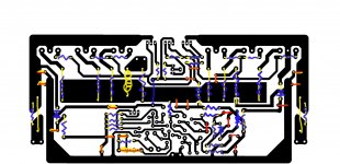
I etched the board and soldered in the components, it took me about 4 days to do this, I loved the build all the way. Looking forward to using the laser printer method, this board was laid out by hand. Also love the community that designed and release something wonderful like this for me to enjoy.
This amp worked right out of the box, I sent 10 volts on a dual supply, 1 amp max output. It worked and seemed to have lots of gain, had the MP3 player on volume 2… When pushed it distorted due to supply voltage. I set the voltage to 27 volts 1 amp supply and again it worked better, the transistors seemed to heat normally and could run like this for quite a while. I measured the current draw at 10mA
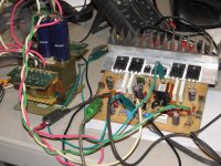
I upped the power supply to 32 volts 4-5 amp max draw… and added two 10,000 uF capacitors to the power supply. The amp worked perfect and sounded pretty good, base was still lacking at this point and the output transistors heated quickly and I had to shut it down 45 sec in. Transistors are mounted on a large insulated heatsink. I measured the current draw at 3.87 per side. Voltage was 32 volts then dropped to 17 when connected to the amp, volume did not change voltage or current draw by more than just a fraction.
Variables – I am using two 2SC5200 & 2SA1943 transistors and MJE15034 & MJE15035 ALL component values are identical to the ones published except for input capacitor (I have .47 instead of 1 uF) and I guessed on the output coil. My estimate would be the coil is probably closer to 2 uH instead of 1.
Any ideas of this overheating problem?
I do not hear any oscillation but input gain seems high. I have some noise when 100k volume is turned down, less volume more input noise.
Thanks,
Pat
I etched the board and soldered in the components, it took me about 4 days to do this, I loved the build all the way. Looking forward to using the laser printer method, this board was laid out by hand. Also love the community that designed and release something wonderful like this for me to enjoy.
This amp worked right out of the box, I sent 10 volts on a dual supply, 1 amp max output. It worked and seemed to have lots of gain, had the MP3 player on volume 2… When pushed it distorted due to supply voltage. I set the voltage to 27 volts 1 amp supply and again it worked better, the transistors seemed to heat normally and could run like this for quite a while. I measured the current draw at 10mA
I upped the power supply to 32 volts 4-5 amp max draw… and added two 10,000 uF capacitors to the power supply. The amp worked perfect and sounded pretty good, base was still lacking at this point and the output transistors heated quickly and I had to shut it down 45 sec in. Transistors are mounted on a large insulated heatsink. I measured the current draw at 3.87 per side. Voltage was 32 volts then dropped to 17 when connected to the amp, volume did not change voltage or current draw by more than just a fraction.
Variables – I am using two 2SC5200 & 2SA1943 transistors and MJE15034 & MJE15035 ALL component values are identical to the ones published except for input capacitor (I have .47 instead of 1 uF) and I guessed on the output coil. My estimate would be the coil is probably closer to 2 uH instead of 1.
Any ideas of this overheating problem?
I do not hear any oscillation but input gain seems high. I have some noise when 100k volume is turned down, less volume more input noise.
Thanks,
Pat
You wont hear oscillation as it is often at a frequency well out of the normal hearing range.
Check R28 with no input and see if it is getting hot. If it is, the circuit is oscillating.
Also check that you have biased the amp correctly. I noticed this is not described in the guide. First set P1 for maximum resistance, then connect a voltmeter on millivolts range across R26. The output bias current is given by (R26*voltage) so for example 6.6mV would correspond to 30mA of bias. You should see a little more than twice this being drawn from the supply when the amp has no input.
I’m sure it has to do with the biasing. I set P1 to 160 ohms like schematic said and that’s it. Everything on the amp seems to work fine when ran at lower voltage.
I just measured R26 at 11mV with bias set all the way at 500 ohms. Then I cranked bias and this changed to 12.9mV
I also pulled the fuse and measured 29.8v across the 100 ohm resistor, after several moments of running the resistor got hot and I had to shut it down.
The input was shorted but I just jumped + and – input, Do I need to also short it to ground also?
My biasing does not seem right this should be around 2.5 mV right?
Here are pictures of my amp, I cant post here yet due to missing security ring? Think I am too new.
http://www.facebook.com/media/set/?set=a.3276583403607.154306.1538131495&type=3&l=f81c481481
I also used these vids to help set measure my results.
http://www.youtube.com/watch?v=cSnBgqo9CS0&feature=related
http://www.youtube.com/watch?v=Ku-w-WAxHs8&feature=related
Any ideas of what I should do next with this bias?
Thanks,
Pat
From your pictures, you have substituted that NTE375 in place of the bias device BD139. The TO-126 and TO-220 devices have different pinouts - one is the reverse of the other.
Also your 2SA1943/2SC5200 transistors look like they may be cheap copies or fakes. If so, that could be causing the oscillation.
Also your 2SA1943/2SC5200 transistors look like they may be cheap copies or fakes. If so, that could be causing the oscillation.
Thanks, this site and the members are the best...
I was doing some recherché last night and discovered that minimally I would have to use a different bias setup due to the transistor change using NTE375 would be different than the original schematic. I did not check pin out though and that will be the first place that I start today. When I asked the local electrical store for a BD139 sub you would think things like reversed pins would stand out in the cross book… a sub should be equal to or better than the original device… but that’s not what NTE cross does…
Thinking I might use a MJE15034 or MJE15035 because that’s what I have left to use… I will certainly order a bunch of BD139, seems like it’s a favorite of many designers. My bias will still be off and I may have to play around with values to get the right mV setting if I use one of the MJE (correct npn or pnp of course I have to look it up)
Once I have the correct gain THEN I will find out if these are fakes or not… I was concerned upon ordering them, I know fakes exist and probably should not have ordered from Ebay even though it was a US seller.
I would appreciate further comment if someone can indeed tell if these transistors are fakes due to what they see.
Its been years since I picked up the soldering gun, I’m pretty happy with the results so far and the fact it worked right away… and now I will learn more while getting it to work right… the learning is what I am after and its been good so far.
Pat
Scratch that, a quick look and the best choice is the MJE340 as bias transistor replacement, and I have those.
The amp works much better now in this configuration…. A good catch, thanks!
Now I am sending 31.2v per rail and 20k storage caps everything is cool with inputs crossed.
The 100 ohm across removed fuse is not hot and I measured 3.2 volts so that gives me 32mA.
Then I measured bias voltage at 7.3mV across 0.22 ohms resistance = 33mA.
I then played music and it distorted pretty quick. I adjusted bias on the fly until it sounded good, this is at the halfway point pretty much like the schematic stated.
I am still not sure what bias voltage I am trying to achieve with these given values?
Last I measured the 5200 & 1943 base to emitter voltage… The NPN had 590mv and the PNP 630mv. After bias I will need to check offset voltage these should be the same right?
Pat
I understand that, what I don’t understand and can’t seem to find is the recommended bias setting voltage or current for this particular amplifier, checked the Blame site, Youtube and this forum. I found that the MKIII should have 1mv bias voltage but I’m wondering if somebody knows this Blame supercharged amp or not.
OR is their some rule of thumb on adjusting bias of an amp… JAYCEE said “You should see a little more than twice this being drawn from the supply when the amp has no input.”
OK so if bias is 30mA then draw should be 60-80 mA but what is the starting bias current of the gain? Adjusting gain will vary the supply current as it should.
So here is a funny story and maybe a lesson too, I needed thermal past for the transistors and ran to the local box electronics store… purchased thermo past designated for computers and lathered up all to the transistors and insulators then mounted them tight. Well for those who know the moral of this story
CPU past is made with silver and is HIGHLY conductive… luckily I checked resistance prior to applying power… I had to replace the insulators and clean each transistor with alcohol to remove that awful sticky stuff… What a mistake…
Pat
Think of the bias current as the idle speed of an engine. The correct way to measure bias current is to measure the voltage drop over one of the output emitter resistors. This will show you the current flowing through that transistor by V=IR. As there are two pairs of output transistors, your total bias current will be twice that.
The adjustment and measurement should be made with no output load, and with the input connected to ground.
The point of bias current is to avoid crossover distortion - that is, the point around which one pair of transistors turn off, and the others on the opposite rail turn on. How much bias current to use is somewhat subjective. I personally use 30mA.
I suspect you still have oscillation issues. Debugging those requires an oscilloscope. A quick indicator of oscillation though is that the Zobel resistor, R28, will get hot.
Thanks Jaycee
I do have a scope, digital dual channel 100mhz... so I'll take a look and see if their is anything strange... Actually this amp is working pretty good right now, its not overheating after an hour of use but I wanted to be certain of the ACTUAL bias current setting (if their is an actual calculated setting according to the designer)... I saw quite a few people setting OTHER amps to 30mA (For now I'll take that as a rule of thumb should the designer or schematic not call it out)...
Your catch on the incorrect bias transistor has seemed to solve the overheating problem")
I’ve been through electronics but this advice is great bringing me back into the game. I wish to build several amps but I need to know everything on how this blame circuit works first. I’m reading Self’s book (or least trying to)
You have taught me Bulb tester, gain current and voltage measurements, idle current, oscillations. Thanks, that’s a great start for me.
NEXT I need to measure offset voltage, understand WHERE to take this measurement, what I am looking for, and HOW to adjust if it’s incorrect.
If anyone cares to have dialog on this issue I’m all ears…
Pat
I do have a scope, digital dual channel 100mhz... so I'll take a look and see if their is anything strange... Actually this amp is working pretty good right now, its not overheating after an hour of use but I wanted to be certain of the ACTUAL bias current setting (if their is an actual calculated setting according to the designer)... I saw quite a few people setting OTHER amps to 30mA (For now I'll take that as a rule of thumb should the designer or schematic not call it out)...
Your catch on the incorrect bias transistor has seemed to solve the overheating problem
I’ve been through electronics but this advice is great bringing me back into the game. I wish to build several amps but I need to know everything on how this blame circuit works first. I’m reading Self’s book (or least trying to)
You have taught me Bulb tester, gain current and voltage measurements, idle current, oscillations. Thanks, that’s a great start for me.
NEXT I need to measure offset voltage, understand WHERE to take this measurement, what I am looking for, and HOW to adjust if it’s incorrect.
If anyone cares to have dialog on this issue I’m all ears…
Pat
Offset voltage is basically the voltage on the output, when the input is zero volts. You will have a little bit of this. In practice, as long as it's under 200mV it's nothing to worry about.
Numerous things influence the offset voltage. Commonly, it is caused by slight mismatches in the devices used in the input stage (Q1 and Q2 in the DX Blame). Some amps do contain adjustments to eliminate it - some use a servo stage with an opamp as an integrator to remove it. Other amps just assume the offset is negligible. On the DX Blame, there's no adjustment for it.
So if you want to measure it, short the input to ground, and use a multimeter on DC millivolts to measure the speaker output. As long as it's below 200mV it's ok. If it's over that, you may want to try matching the hFE of Q1 and Q2.
That sounds pretty easy. I thought offset was the difference between the starting points of the positive cycle compared to the negative. I thought you had to measure it in the small signal section then adjust one side of the NPN or PNP side of the transistors… Kind of hard to explain here without paper…
I sat down with the amp today and finally gave it a proper sound audio test… This thing works great… sounds wonderful and is producing very small amounts of heat; I ran it wide open for 5 hours and no problems. Other builders may be interested to know I am using MJE3055T & MJE2955T for Q9 and Q10 then a MJE340 for bias transistor Q8. And the final output transistors Q11-Q14 are 2sc5200 & 2sa1943… I blew out Q9 & Q10 with a slip of my meter probe and had to use what I have on hand… Still works great and sonically sounds pretty good.
I’m thinking after a bit more of reading I will build another one… This time I will use the laser toner transfer method for making the PC board instead of laying it out by hand and I will make two at a time, left and right. Before printing the boards I wish to Photoshop the design and include one more NPN and PNP output transistor on each side. I BELIEVE that I can do this without modifying any other value or part on the board. Just make the board a little wider, move the pos and neg traces out to the sides and insert another transistor and resistors R23 & R26…. I will use MJL4281A & MJL4302A and everything else like the original schematic. All amps I build need to be PA rated so for overkill I would like to include another set of transistors.
Also I couldn’t resist and opened up one of the transistors 2sc5200 to look at the die size… its pretty much junk 1.5mm x 1.5mm die… I knew these transistors were not Toshiba but I figured it was a third party COPY with similar or same specifications… sadly its not. Its working great right now but the next amp will have new transistors for sure.
Pat
Attachments
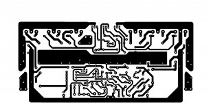
I was thinking of something like this… I would call it DX Blame MKII Super Duper Supercharged amp… 1 extra set of output transistors…. I CAN DO THIS RIGHT?
The final layout will come once I have all the parts on hand so I can tweak the layout should a capacitor or fuse socket need just a bit more space.
I would power it with 45 volts (61 after regulation) 300VA transformer per side and make all the capacitors rated at 100 volts (80 volts for the storage caps 60,000uF total each amp)
Design goal would be 150 Watts output at 8 ohms for use in PA application of top high and mid speakers.
What do you think?
Attachments
Last edited:
Here is all you need: Amplificadores DX Blame - Carlos Mergulhão
Click on DX Blame Supercharged link and there you go - Schematic , PCB normal and inverted for the toner transfer method and two pairs of outputs and of course size of PCB.
Regards!
Click on DX Blame Supercharged link and there you go - Schematic , PCB normal and inverted for the toner transfer method and two pairs of outputs and of course size of PCB.
Regards!
Member
Joined 2009
Paid Member
Should be no problem to change it up with an extra pair of outputs. The thing with multiple outputs is that for good current sharing between these devices you want to ensure the devices are 'matched' so that they all turn on together and flow similar current. This usually means buying extra and testing them - something I've never done because I'm too lazy. Although I've never tried it, I think multiple output devices from the same batch will be fairly well matched already and then just use largish emitter resistors, say 0R47 to force the current sharing a bit more.
Nice build by the way. It was about 3 years ago I started my first amplifier (called TGM) along very similar lines to you. There's always something to learn with these projects, whether it's choice of parts, optimizing the circuit with a 'scope, finding and fixing a problem, layout out pcb, designing a better power supply, etc. A very enjoyable experience for the most part. For me, the experience was incomplete without building a speaker to go with the amplifier, something relatively simple from the Full Range forum.
I hope you realize that this hobby is very addictive
p.s. I noticed in your photo that you have a simple carbon-track open potentiometer for bias adjustment. A lot of older amps used them. The trouble is they can degrade over time, depending on their quality, so I use only sealed potentiometers and I use mult-turn types to make adjustment easier.
Last edited:
- Status
- This old topic is closed. If you want to reopen this topic, contact a moderator using the "Report Post" button.
- Home
- Amplifiers
- Solid State
- Overheating on NEW DX Blame super