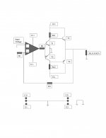
This is a schematics which I think I have just invented but I am not sure whether the circuit has not been invented before. This circuit uses a common emitter connection of the transistor(s) T1 and T2 and a common collector connection with the transistors T3 and T4 and the operational amplifier acts as a transistor stabiliser and source. In other words, the “analogue logic is carried out by the operational amplifier and the power as well as voltage conversion is carried out by T1, T2, T3 and T4. The most important application of this circuit is where the operational amplifier (whether buffered by power transistors in the feedback after the IC output or not) cannot provide the necessary output voltage because of the limitations of the maximum supply voltage of the operational amplifier. Hence, a separate power supply can be connected through resistors Rc1 and Rc2 to the collectors of T1 and T2 (common emitter) and without any resistors to the collectors of T3 and T4 (common collector). The beauty of this circuit as opposed to the standard common emitter or collector discrete transistor amplifier circuits is the feedback is after the transistors and therefore the output voltage does not depend on the transistor circuits but on the ability of the operational amplifier to maintain the voltage on the plus input to be equal to the voltage of the minus input, which ability is rather high. Also, the output impedance of the whole circuit with transistors before the feedback is much lower than the output impedance of a common collector amplifier built as a separate circuit and not related to the operational amplifier (i. e. positioned after the feedback).
Basically this whole circuit is a simple externally boosted operational amplifier. The output voltage can be bigger than the range of the operational amplifier but this is not a problem because this output voltage will be divided and the result of the division will be and must be within the range of the operational amplifier. Rb can be omitted physically, and, for simplicity, these explanations will be provided when Rb=0 is assumed. Thus the operational amplifier IC output pin will swing between -0.7 and +0.7 running T1 and T2 and depending on the voltage current characteristics of their base emitter junctions for control. Rb can be inserted in order to enlarge the control range and thus reduce the sensitivity of the control but the well feedbacked operational amplifier will be able to maintain the necessary base emitter voltage even without Rb because of the high level of precision of the control ability of the operational amplifier. As depends on the IC’s output pin voltage, one of the transistors (T1, T2) will go more open or more closed whilst the other one does the opposite: goes more close or more open. THE IMPOSTANT THING TO NOTE IS THE EMITTERS OF T1 AND T2 ARE CONNECTED TO GROUND WHICH GIVES THE OPERATIONAL AMPLIFIER TO CONTROL THESE AS THE IC PIN OUTPUT VOLTAGE IS REFERENCED TO GROUND AND NOT TO U2+ NOR U2- WHICH VOLTAGES (U2+ AND U2-) THE OPERATIONAL AMPLIFIER MAY NOT BE ABLE TO ACHIEVE AT ALL. Operational amplifiers have a limit of the maximum supply voltage due to internal design limitations (unless the operational amplifier has been specifically designed to work under hifgh supply voltage in which case, some parameters y have been sacrificed to have achieved this ability). For example, the iconic TL084 has been designed to be able to perform with maximum +/- 18V supply voltage (U1+=18V max and U1-=-18V min). TL)84 is not rail to rail amplifier and there isn’t a true rail to rail amplifier as far as I know although the companies would call them so because there is just a tiny bit more to go to become real to reel (real reel to reel). Usually, the operational amplifiers would go all the way down to negative but will be shy of a bit to reach the positive supply reel. TL084 can go from negative to positive -1.5V. In case of maximum power supply of +/-18V, TL084 would be able to go from -18 to + 16.5V at the IC output pin. When symmetry is needed, TL084 would be able to swing the output (to wave the dick on the beaches of Florida) from -16.5V to +16.5V. A perfect sine with an amplitude of 16.5V would have an RMS value of Amplitude * 0.707 which, in this case, is approximately 12V. The square of this RMS value divided by the load resistance RL would give the maximum power a circuit with output of +/-16.5V in amplitude would be able to give even when no limitation of the maximum current exist. Thus, a 4O loudspeaker will suck twice as much power out of an amplifier with a given output voltage as an 8O loudspeaker ONLY IN CASE THE AMPLIFIER CAN PROVIDE THIS POWER, i. e. maintain the voltage while blowing a current with an RMS value of 12VRMS/4O=3A. An amplifier with a +/-16V output will then be able to provide a maximum of 36W RMS when connected to a 4O speaker. REMEMBER: THE AUDIO AMPLIFIER IS A VOLTAGE SOURCE NOT A CURRENT SOURCE. THE AUDIO AMPLIFIER GIVES A VOLTAGE AND TRIES TO DO THE BEST POSSIBLE TO MAINTAIN THIS VOLTAGE AT ANY CURRENT SUCKED OUT OF THE AUDIO AMPLIFIER TO THE MAXIMUM CURRENT POSSIBLE. I.E. AUDIO AMPLIFIER WORKS IN REGIME OF A MAINTAINED VOLTAGE NOT IN A REGIME OF A MAINTAINED CURRENT.
So, is there any way to have an amplifier with maximum amplitude +/- 16.5V to give more power when a load of 4O is connected? NO! There is only one way. Get more voltage. But the operational amplifier does not allow for more voltage. Then run the operational amplifier up to this voltage and build a circuit controlled within this range which can give more voltage because the circuit will be supplied by a higher voltage while only controlled by the lower voltage possible to be achieved by the operational amplifier. So, put, say +/-5V supply to the operational amplifier (whichy will be able to reach a symmetric output of +/-3.5V and then build a separate common emitter circuit which will be supplied by, say +/-60V and will run the loudspeaker. Or you may not have an operational amplifier at all. However, the circuit with an operational amplifier and a feedback after the power transistors has a lot of advantages previously discussed.
The common emitter connected T1 and T2 amplify and invert the signal of the operational amplifier and display this at their collectors which, in turn, drive the common collector followers T3 and T4 for which reason Rc1 and Rc2 must have such values as to allow the necessary current to fly through the base emitter junctions of T3 and T4. T3 and T4 do the opposite “ground : supply” consideration: while T1 and T2 take one signal, reference this signal to ground and split (“uncombine”) the signal to provide two outputs at their collectors, T3 and T4 take these two outputs as their inputs, reference these to U2+/- (T3 to U2+, T4 to U2-) and combine them again into one output which goes to RL.
The output voltage at RL will be much higher than the operational amplifier can handle. This means, there will be periods when the operational amplifier will go in saturation and will not be able to provide control and the same will happen to the output. This is why, the R2, R1 arranged feedback divides this output voltage to bring the input voltage coming from the output through the feedback in a size possible to be handled by the operational amplifier. When ground is applied to the negative input, the operational amplifier will do such as to have 0V on the positive (virtual ground). Thus a cureent of Uin/R1 will fly through R1 which can go nowhere but through R2, thus the output must be adjusted by the IC in such a way as to allow this same current to fly through R2. But one of the ends of R2 is connected to the positive pin (virtual 0V) which has 0V because the negative is connected to ground and the operational amplifier does nothing else but adjusting the output to make the two inputs equal. The other end of R2 is connected to the output Uout. Therefore Uout must be adjusted by the operational amplifier to be:
Uout/R2=Uin/R1
In order to have the current fly through, or to “suck” the whole current to the output.
Rewrite the formula:
Uout/Uin=R2/R1 which is:
Uout=Uin R2/R1
So, the output is equal to the input multiplied by a coefficient R2/R1 which coefficient is the gain G=R2/R1. NOTE: BECAUSE OF THE R2, R1 FEEDBACK Rc1/2 DO NOT HAVE ANYTHING TO DO WITH THE GAIN.
Will the operational amplifier be able to adjust the output this way? Assume the input Uin is positive, then the current flies from Uin through R1 to the positive pin (virtual ground), then cannot go nowhere else except through R2 and then continues to the output to pass through RL in part and through T4 to negative power supply U2- and then through the U2 power supply to the common ground between U2 U1 and Uin which must exist otherwise voltages will fly all over the place without any reference with each other.
In order for this current to be able to fly, the operational amplifier must adjust the output voltage to be negative and with a certain value. Because the operational amplifier is feedbacked, the operational amplifier will be able to provide the value of this voltage for sure as long as the feedback is stabilising and not generating feedback, means negative and not positive. This is the ONLY condition for feedbacked systems (the only qualitative (logical) condition, not quantitative (amount of how good the feedback is)). (This can easily be explained but not now.)
So, do we have a positive or a negative feedback? The only thing which can say so is the signs of the input and the output. In case the signs are the same, we have a positive feedback, otherwise, we have a negative.
Yes, but the feedback goes to the positive pin, this means positive?!? In most cases, yes but, not in this case. The output of the IC is INVERTED by the common emitter then REPEATED (not inverted) by the common collector. Therefore, the output of the schematic is inverted as compared to the output of the IC. Assume, we follow the standard procedures and put the feedback to negative. Then the IC will invert Uin the same way as the standard inverting operational amplifier circuitry does. Then the common emitter will invert again. Therefore Uout will have the same sign as Uin. Now, assume we connect the feedback to the positive pin (as shown). Then the IC does NOT invert the signal but the common emitter does, so the output Uout is opposite in sign to the input Uin which means we have a NEGATIVE (STABILISING) FEEDBACK although we connect to the positive pin. This is because we have an inverter immediately after the IC and before the point where the feedback is taken from.
Generally, this schematic is the SAME as the standard inverting amplifier as far as the logic of the way the schematic works is concerned, just there is an invertor at the end of the operational amplifier thus the feedback must go to the positive pin.
The same schematic may be connected to the equivalent way and logically the same as the standard noninverting amplifier, then point of R1 where Uin is applied now must be grounded and Uin must be applied at the positive pin. The derivation of the formula for the gain is the same as the derivation of the formula of the gain of the standard noninverting amplifier and the gain is: G=1+R2/R1
Any ingenious design? No. The circuit is the same as:
a) The standard amplifier, just the output is additionally inverted and more powerful and takes different power supply, yet has a SINGLE GENERAL FEEDBACK which gives the best parameters possible at the huge power output.
b) The standard amplifier with boosted output with common collectors, just the output is inverted and power is taken from a separate power source
c) The separately built circuitry by a standard operational amplifier, a separate common emitter and a separate common collector each of them with their own feedback wherever whatever necessary. (Common emitter does NOT require an AC FEEDBACK only DC. Common emitter is straight, non regulated amplifier.) The parameters of this circuitry will be worse.
d) Same as c) but with a general feedback as well as separate. Works OK but the parameters will not be as good as single general feedback. Mainly the speed of control as far as I can think. This is also because the straight gain will be lower which also leads to higher output impedance and lower input and is a fuckin’ waste of components and assembly.
Anyways much ado for notha. Also, much a do for notha. I have not though carefully through this schematic, so you must.
Attachments
I am in a hurry. I copied and pasted from another document written for another purpose. Have not checked the schematic perfectly although the schematic is pretty simple and basic. Have not made the circuit yet. Considerations similar to the post of a Pre Amplifier which I have done on this site in another thread. I must hurry up now. Comments and suggestions as well as mistake corrections are welcome.
Not read everything, but the scheme is known (at least) since the mid-seventies.
W Jung mentions it in his book "Op Amp applications handbook" (p590), and there are other references, here for examples:
http://www.ti.com/lit/an/sboa009/sboa009.pdf
In the seventies, the topology was used in low cost car amp boosters, to drive a 2 ohm load rail-to-rail.
W Jung mentions it in his book "Op Amp applications handbook" (p590), and there are other references, here for examples:
http://www.ti.com/lit/an/sboa009/sboa009.pdf
In the seventies, the topology was used in low cost car amp boosters, to drive a 2 ohm load rail-to-rail.
Thanks.
I have expected to have been made long ago. To "defend" the case I would say what I have said: "I just invented this circuit but this circuit may have been invented already."
I personally believe neither I nor Jung nor anyone else has ever invented this circuit because there is nothing to invent. Or, in case we want to find an inventor, this may be De Forester.
This is a basic end of any amplifier or operational amplifire. More, this is a basic common emitter and common collector with a general feedback whether with an operational amplifier or without. Another inventor may be the inventor of the general feedback dated a few million years ago when the monkeys became human or even before.
However, I do believe the circuit is kinda nice and useful. What I like the most is so an operational amplifier based circuitry can take care of the analogue logic in case there is such and then the "output portion" of the operational amplifier can be repeated in order to change to common ground and then again to common load thus allowing for another external voltage (possibly huge) to be applied to the circuit and displayed at the output in a "maintained voltage" fashion, thus doing the dirty job while the operational amplifier does the white collar job, and the too jobs can be feedbacked (combined) one with another using a ralatively simple general feedback with a huge gain in the straight track.
What a fantastic explanation of a lousy common emitter and common collector invented millions of years ago and applied in electronics when the first tubes arrived.
However, there is something interesting: The circuit cannot work as a follower (buffer) because the output voltage must always be greater than the input (unless the same or lower (be careful with attenuation, cannot think now whether more compensation of the operational amplifier may be needed or not) in some specific cases whether there are such applications or not) as far as I can think now and I haven't given a great deal of thought.
In applications where infinite input impedance is necessary, a separate buffer is to be put before the general feedback.
However, assuming we can put 36V to TL084 and assuming we want to put, say 100V at the output, we look at an additional gain of 3. The general feedback will be still deep enough and we will still get rather enourmous input impedance and a tiny output impedance.
Again: one of the problems with this circuit, as far as I can see, is the necessity of dual power supply. In some countries power supplies (at least simple transformers) are available almost for free. Also, kits are sold for pennies and people wind them themselves. In other countries, lousy pieces of inexpansive laminated rusting iron or still woth 1c or less and a few grams of copper worth less or close to the equivalent number of pennies which make the load (pennies are made out of copper, ain't they) cost $100 and up. They can import these from China but not very many do not because they want to keep them jobs around but because power transformers are big and cost more money to ship them from China to elsewhere.
Anyways, by saying "invent" I meant I had done the circuit without knoing anyone else has. I prefer to reinvent the wheel instead of reading Jung or Junk.
Y'all may wish to do the same and your designs would work better (I am sure they do anyways). Problem orientation may help.
Not read everything, but the scheme is known (at least) since the mid-seventies.
W Jung mentions it in his book "Op Amp applications handbook" (p590), and there are other references, here for examples:
http://www.ti.com/lit/an/sboa009/sboa009.pdf
In the seventies, the topology was used in low cost car amp boosters, to drive a 2 ohm load rail-to-rail.
Sorry, I forgot to undeline: I think the problem with COMMON GROUND to COMMON LOAD conversion is very important to be thought of THEORETICALLY in a general theoretical thinking, not with this schematic only but in general, from the point of view of electrical techniques not from the point of view of electronics regardles of whether this can be achieved with active electronics only or not.
Someone may need this somewhere.
Someone may need this somewhere.
Also, why only car amplifier (where the voltage is the same unless they boosted it up bu DC to AC, step up transformern AC to DC or whatever other way the may have found), why not guitar?
I might have mixed things up: there were several variants of this booster, all ending with big common emitter BJTs on each rail.
In some cases, the bases were driven directly by the amp supply rails, in others there were drivers between the amplifier and the OP devices.
There are some commercial examples of higher voltage amplifiers utilizing a similar scheme.
Other members will probably have clearer recollections than mine.
You did not but I missed the point(s) you made clear. Anyways, I was mainly interested in displaying higher voltage than the supply limit of the operational amplifier at the output.
However, I am proud there was some kind of application in the '70's cars. The only real cars so far.
However, I am proud there was some kind of application in the '70's cars. The only real cars so far.
It's quite commonly used as a headphone amplifier, with the opamp driving the transistors via biasing diodes. In this case T1 and T2 act as the biasing diodes.
A much better use of T1 and T2 is if they are connected in what is known as the Diamond Buffer configuration. This is what I use in my own headphone amplifier.
A much better use of T1 and T2 is if they are connected in what is known as the Diamond Buffer configuration. This is what I use in my own headphone amplifier.
Headphones do not require power. A simple common collector couple (standard boosting of an operational amplifier output) connected to the same power supply as the operational amplifier would do or just the operational amplifier driving 50mA max through the headphones as depends on the power supply and, bad news, the resistance of the headphone speakers. Thus 36V power supply to TL084 would allow TL084 to swing -18 to 16.5V, to keep the symetry: -16.5 to 16.5 which is 16.5*0.707~12V RMS. I do NOT know how big the resistance of the headphones is. In case of 240 Ohms, then you get the maximum of 0.6W. In case higher, you get less power. In case lower, you must lower the supply voltage (or play it risky and rely you don't push the gain too much for the applications you want) and still get less power.
Another thing I do not know is what "Diamond Buffer" is but this may be the same to what I referred to as "common collectors at the output of the IC". I do NOT want to look up right now because I do NOT like terminology.
Another thing I do not know is what "Diamond Buffer" is but this may be the same to what I referred to as "common collectors at the output of the IC". I do NOT want to look up right now because I do NOT like terminology.
Sorry, in case of high resistance you best go to another supply but do you believe the resistance would be much higher than 240? Or much lower? In case of no, do you not believe 0.6W or even 0.1W is good enough for headphones?
I do not object your idea, I just do NOT know how big the resistance of headphones is (believe to be much higher than 4, 8, 12 even 16 Ohm speakers), so I cannot calculate the power and I do NOT know how much power is needed for headphones.
I do not object your idea, I just do NOT know how big the resistance of headphones is (believe to be much higher than 4, 8, 12 even 16 Ohm speakers), so I cannot calculate the power and I do NOT know how much power is needed for headphones.
A couple of questions about the circuit. As I see it, the first pair of transistors will be "cut off" i.e. no current through them. Then all the current through the resistors rc1 and rc2 will flow through the bases of the second pair. The second pair must operate in "class A" mode, since there has to be enough base current drive to deliver current to the load. So will be hot. Also, as output devices heat up, Hfe goes up and current increases, ie thermal runaway. Still trying to "wrap my mind" about what goes on in the output - how much drive do you need to be able to get output to near the rails with a load. Interesting circuit ...
A straight protection can be achieved with a couple of zeners just before the feedback. These will protect the speackers but will straight connect the transisrtors. Higher voltage zeners can be put just in case. The leackage is not important neither is their non linearity because they are before the feedback.
A simple zener couple to limit the output.
Forgot the circuit. Need to recall.
A couple of questions about the circuit. As I see it, the first pair of transistors will be "cut off" i.e. no current through them. Then all the current through the resistors rc1 and rc2 will flow through the bases of the second pair. The second pair must operate in "class A" mode, since there has to be enough base current drive to deliver current to the load. So will be hot. Also, as output devices heat up, Hfe goes up and current increases, ie thermal runaway. Still trying to "wrap my mind" about what goes on in the output - how much drive do you need to be able to get output to near the rails with a load. Interesting circuit ...
What you say looks 100% true. However, the second pair of transistors are in common collector connection. Look at the upper half of the schematic only for simplicity. The left hand side transistor is in commen emitter. The right hand side is in common collector. The inverted voltage of the input of the common emitter would be limited ( " cut off " ). Thus the voltage supplied to the common collector gets limited ( " cut off " ) too. The 100% feedback of the common collector will not allow any high current to go through because the voltage of the output ( emitter) must be maintained to be the voltage of the input ( base ). The transistor would open and close accordingly to maintain this voltage. The end transistor, basically, is a common collector with all the load in the emitter as opposed to having the load in parallel to Re.
A couple of questions about the circuit. As I see it, the first pair of transistors will be "cut off" i.e. no current through them. Then all the current through the resistors rc1 and rc2 will flow through the bases of the second pair. The second pair must operate in "class A" mode, since there has to be enough base current drive to deliver current to the load. So will be hot. Also, as output devices heat up, Hfe goes up and current increases, ie thermal runaway. Still trying to "wrap my mind" about what goes on in the output - how much drive do you need to be able to get output to near the rails with a load. Interesting circuit ...
- Status
- This old topic is closed. If you want to reopen this topic, contact a moderator using the "Report Post" button.
- Home
- Amplifiers
- Solid State
- Simple Amplifier