alternative ?
post #1569
http://www.diyaudio.com/forums/solid-state/193923-simple-symetrical-amplifier-157.html
post #1569
http://www.diyaudio.com/forums/solid-state/193923-simple-symetrical-amplifier-157.html
Attachments
I'm not sure about that. The Vbe multiplier does not need to be on the same heatsink as the output drivers, but it still needs to track the temperature of the pre-drivers.
I agree with this.
Not tracking works in this circuit because the drivers' temperature is relatively stable if the Vsupplies are not too high..
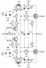
Here is the circuit (apologies if I transgress a forum rule about other people's circuits).
Note that this circuit is for the p3, not the p3a.
Last edited:
Well, you just showed us the confusing part with Randy's descriptions. He uses "output driver" instead of the more familiar "output transistor" and "pre-driver" for driver etc. If you get a laugh out of the term "pre-pre drivers" used in triples, he sure uses that one too!...The Vbe multiplier does not need to be on the same heatsink as the output drivers, but it still needs to track the temperature of the pre-drivers. Randy Slone explains this rather better than Douglas Self - I have just checked....
Randy did strive to simplify but used some oddball terms and expressions in the process. Take care with his text.
He probably took a leaf or twenty from D.Self's book. Who else calls optimally biased ClassAB as Self's ClassB?............. but used some oddball terms and expressions in the process. Take care with his text.
ladies and gents ...let us not forget that the OP is just 15 years old ...there is too much information in this thread in too difficult language, and with many abbreviations to understand for 15 year old with probably little experience .
i suggest that some may focus on the OP questions and please keep it in plain ...greek
kind regards
sakis
i suggest that some may focus on the OP questions and please keep it in plain ...greek
kind regards
sakis
a few facts ...( at least from a currently P3A builder )
amplifier like the P3a is sziklai or cfp resulting that if your target is very very high quality the pcb needs to be proper and under some rules .... other amplifiers is similar sensitive but these amps a bit more .
--drivers have to be close to the outputs
---output trace together with collector resistors needs to be tight and organized and as small is possible while away from small signal input transistors
---except 100nf decoupling it could be nice to have together 100mfd /63 volt or more but closer to the outputs while the connection to ground is also as short is possible
--- feedback resistor is to be connected to the output R5 22k if possible just next to the output lead
--- input transistors may be located "face to face " with each other and that will give you the chance to glue them together and make them behave better since they share the same temperature
---miller capacitors C6-C4 need to be of some quality and voltage above 160volts and either mika or styroflex while as close is possible to the transistor connected
--- current source for transistors 1-2 is the transistor Q3 that also needs to be as close to the input transistors 1-2
dont be afraid to use jumper links to achieve your targets ...up to 3-4 is ok ...more is getting away
the Vbe issue TR9 might become critical if you have plans to push the amp around and high temperatures are expected .... in this case you might want to relocate it close to the drivers either glue it to one of them so it senses temperature from .
ideally one heatsink ( small piece of aluminum) that will include drivers Q5-6 and Q9 will be the best hing to do ...Q9 might sense temp from both of the drivers .
In a case the amplifier is for casual listening and not expected to be pushed around none of these is needed but yes the bias will drift depending on the level of sound and the room temperature still you might get away with it
remember to use a big heatsink just o be on he safe side ....
if you have any other questions please post here and i will do my best to keep it simple
kind regards sakis
Last edited:
ladies and gents ...let us not forget that the OP is just 15 years old ...there is too much information in this thread in too difficult language, and with many abbreviations to understand for 15 year old with probably little experience .
i suggest that some may focus on the OP questions and please keep it in plain ...greek
kind regards
sakis
Thank you sakis! I really needed this thing! This language was too hi-fi for me!
a few facts ...( at least from a currently P3A builder )
amplifier like the P3a is sziklai or cfp resulting that if your target is very very high quality the pcb needs to be proper and under some rules .... other amplifiers is similar sensitive but these amps a bit more .
--drivers have to be close to the outputs
---output trace together with collector resistors needs to be tight and organized and as small is possible while away from small signal input transistors
---except 100nf decoupling it could be nice to have together 100mfd /63 volt or more but closer to the outputs while the connection to ground is also as short is possible
--- feedback resistor is to be connected to the output R5 22k if possible just next to the output lead
--- input transistors may be located "face to face " with each other and that will give you the chance to glue them together and make them behave better since they share the same temperature
---miller capacitors C6-C4 need to be of some quality and voltage above 160volts and either mika or styroflex while as close is possible to the transistor connected
--- current source for transistors 1-2 is the transistor Q3 that also needs to be as close to the input transistors 1-2
dont be afraid to use jumper links to achieve your targets ...up to 3-4 is ok ...more is getting away
the Vbe issue TR9 might become critical if you have plans to push the amp around and high temperatures are expected .... in this case you might want to relocate it close to the drivers either glue it to one of them so it senses temperature from .
ideally one heatsink ( small piece of aluminum) that will include drivers Q5-6 and Q9 will be the best hing to do ...Q9 might sense temp from both of the drivers .
In a case the amplifier is for casual listening and not expected to be pushed around none of these is needed but yes the bias will drift depending on the level of sound and the room temperature still you might get away with it
remember to use a big heatsink just o be on he safe side ....
if you have any other questions please post here and i will do my best to keep it simple
kind regards sakis
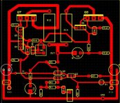
I've edited the layout to some extent keeping your points in mind and i hope that I haven't f**ked it up!!
I found a thread having the P3A Layout.I verified the layout with the schematic and i'm thinking of going with this layout...I seriously am not worth designing layouts! I need to observe professional layouts and then start designing my own!
Till then, i'll take ideas from this thread!
http://www.diyaudio.com/forums/solid-state/183234-esp-p3a-3.html
Thanks a lot for your help. I'm really grateful to...!
In the mean time, I am designing Rod's P27 Amp's Design in which i'm trying to keep the same layout as Rod's layout..I'm on the verge of completing it..I'll start a new thread for it's layout and get back to you soon.
Regards
Attachments
Hi Paranoid06
Really nice work, one more comment:
A sensitive node (to both pick-up and stray capacitance) is the feedback to the input pair (the common trace(s) connecting R4, R5 and Q2's base).
Try to minimize the copper used for these connections. There are numerous ways including moving C3 with another vertical ground trace.
Have fun and good luck
-Antonio
First thing to do - look at the picture of Rod's board. Even though you can only see the top side, you can see how he has placed components. Use this as a hint.
Traces - use 1.27mm traces all around apart from the power and ground traces - make those as wide as possible, at least 2.54mm wide. The bypass capacitors should also be close to the output devices.
The big looping circle around Q7 from the power rail - shorten it. Take the track from the centre collector pin to the resistor from the other side.
Compensation caps C4/C6 - get them as close to the device as possible. Practically right on the pins. Dont worry about using fancy silver mica capacitors - good NPO dielectric (low K) ceramics will work just as well.
Put Q9 right next to Q5. You can move Q4 away a bit. Keep the TO-220 devices horizontally aligned.
R11-R12 - these feed the drivers, so make the track go from the resistor, to the driver collector pin, and then from the driver collector pin to the outputs base pin.
R9-R10 need to be 1W resistors, so you need a larger part spacing there.
C1 - too small a spacing. I found a Wima MKS2 3.3uf 50v polyester capacitor works well here. That is a pin pitch of 5mm, and a diameter of about 7.5mm. If you want to use an electrolytic capacitor there, that will also fit.
You appear to have left out C2. It's important.
You should be able to use a board thats half the size you currently have. It just takes practice. Expect to lay out the design a good 5-10 times before you get it right, if this is your first attempt at designing a PCB. It was my first attempt too, I think I got to version 6 before I was happy")
Traces - use 1.27mm traces all around apart from the power and ground traces - make those as wide as possible, at least 2.54mm wide. The bypass capacitors should also be close to the output devices.
The big looping circle around Q7 from the power rail - shorten it. Take the track from the centre collector pin to the resistor from the other side.
Compensation caps C4/C6 - get them as close to the device as possible. Practically right on the pins. Dont worry about using fancy silver mica capacitors - good NPO dielectric (low K) ceramics will work just as well.
Put Q9 right next to Q5. You can move Q4 away a bit. Keep the TO-220 devices horizontally aligned.
R11-R12 - these feed the drivers, so make the track go from the resistor, to the driver collector pin, and then from the driver collector pin to the outputs base pin.
R9-R10 need to be 1W resistors, so you need a larger part spacing there.
C1 - too small a spacing. I found a Wima MKS2 3.3uf 50v polyester capacitor works well here. That is a pin pitch of 5mm, and a diameter of about 7.5mm. If you want to use an electrolytic capacitor there, that will also fit.
You appear to have left out C2. It's important.
You should be able to use a board thats half the size you currently have. It just takes practice. Expect to lay out the design a good 5-10 times before you get it right, if this is your first attempt at designing a PCB. It was my first attempt too, I think I got to version 6 before I was happy
Original Symasym thead is here
http://www.diyaudio.com/forums/soli...ifier-designed-michael-bittner-our-mikeb.html
Best of luck
Gajanan Phadte
http://www.diyaudio.com/forums/soli...ifier-designed-michael-bittner-our-mikeb.html
Best of luck
Gajanan Phadte
Yes, and I hope also appreciates that he/she is dealing voltages that, potentially, can hurt or kill. Paranoid06, please read Rod Elliott's pages about wiring and handling mains voltages.let us not forget that the OP is just 15 years old
We don't want an ex-member.
well ...it seems that from the things i told you you have done almost nothing.....
your pcb will work ( produce sound) as is as i said if you are aiming to really high quality sound this pcb cannot go there
jay cee has given you also some useful advice....
--- you use a jumper to supply Q1-2 which is actually ok but proximity between traces is not right .... you can actually do that better
--- Making such a big circle around + rail around the power transistor is not OK ...better with a jumper
--- you forgot to relocate C6
--- you was advised to make Q1-2 go face to face .... it works better for mechanical reasons not one behind the other
--- you was advised to move Q9 close to the driver
--- Finally the all pcb can be rearranged to be more more clean and reorganized see how others did and see what you like to keep
i want to built 2sk1058,2sj162 based amplifier but not availability of pcb i am very nervous .please give me the site name from where i can construct it.
Get hold of Randy Slone's book "High Power Audio Amplifier Construction Manual" and look at the figure 11-1 project. It is based upon the original proven circuit from the Hitachi databook. There is a PCB layout as well.
dear gmphandte,
i want to built 2sk1058,2sj162 based amplifier but not availability of pcb i am very nervous .please give me the site name from where i can construct it.thanking you.
yours ever masood
It could be nice to relocate your request elsewhere in a similar thread cause if a subject like that is discussed here might only bring confusion to our 15 year old friend
kind regards
sakis
From what I can make out, paranoid06 should give up on the original idea and go with a chip amp, probably LM1875 because of lower voltage requirements. This project is too ambitious for someone with clearly limited skills and knowledge and is, potentially, lethal. As it will involve mains wiring, I am unesy about anyway.
paranoid, do your parents understand the dangers?
paranoid, do your parents understand the dangers?
francec ...one way or another both circuits somehow will need to be connected to mains eventually so whats the catch ?
then again the P3a will play by far better than the 1875 .... so give the kid a chance or post a nice article on safety procedures ( many can be found at the end of any elektor magazine )
then again the P3a will play by far better than the 1875 .... so give the kid a chance or post a nice article on safety procedures ( many can be found at the end of any elektor magazine )
sakis, the kid is 15!
His/her parents have a right and obligation to know what their child is up to and the dangers involved. We have an obligation to ensure a young kid is not harmed through our advice. I tempered my comments above by saying I was uneasy with any project that involved mains voltages. In Oz, it is 230V and it kills. I just checked and India is 230V as well.
Purely from self-interest, can you imagine the problems for this forum and us as members if something tragic happened and the kid was acting on OUR advice and was killed. However, that is far less important than ensuring, for moral and ethical reasons, the safety of the child.
Pleas of "give the kid a chance" border on irresponsible and I will treat them with the contempt it deserves. Does the kid properly understand safety issues and the potential of mains voltages to harm and kill? If you can guarantee he/she does, let me know with an ironclad assurance. Otherwise, give advice that is less potentially harmful.
My advice for the kid is to start with a 12V project or with a pre-built power supply that complies with electrical safety regulations.
Frank
- Home
- Amplifiers
- Solid State
- Rod Elliot P3A Layout - Critics