Thank you, Bonsai. I know it is a simple amp , but this is what is needed.
I'm down to just the input cap now ... ahhhhh
As it is , the options include:
- 2 compensation schemes -TMC and standard miller.
- 3 possible input stages- a. Just a simple 2 device input pair , b. a cascoded low noise BJT input pair, or .. c. a cascoded low noise Jfet input pair.
- 3 adjustments - some might say this is excessive.
a. is the main bias control - you ABSOLUTELY need this one to bias the amplifier. b. offset adjust - makes for that final touch of <2mv DC at output.
c. the CCS adjust.- different input pair devices are best optimized at different currents. .7 - 2.5ma (per device) is the range of this control.
- All double- sided traces can be directly jumpered for single- sided construction , this artwork can be used by both the board store and the laser printer madmen.
- Smaller on-board decoupling (1-2.2kuf) with a large external supply , or max onboard of 22Kuf X2. - 470uf VAS/IPS secondary decoupling.
Some said that I should do a triple .... I am for myself , using the same "style" for this board as for my own (output stage nearly the same). Nothing wrong with high beta EF2 , and I would and do own several of this design.
Around 94 components total full cascode , minimum 80 with no tmc/cascode/leds - etc.... 2 years ago I would not of been scared
OS
Attachments
Last edited:
Thank you , hugh. At least someone appreciates an EF2.
I do think this one might exceed the silicon chip LIN amp. Layout is the only factor that can differentiate one ppm amp over another. NFB is dropped to 1/40th of output before it gets anywhere near the LTP/cascodes. some "snake" the full output back to the input stage resistor. I just don't like a 100v p-p right next to millivolts .
I hope you don't mind , but your amp designs (naska) influenced my choice of massive on-board decoupling. I just ported everything to mouser/apex jr./digikey so it could be a "world amp".
The sound might be considered "clinical" by some , but with the FET input option , the right combo of cascode/fet could make for some good sound.
Durability and MTBF , as planned .. nothing beats this amp.. 15- 20 years heavy use , no problem (regrease the OP/recap every decade). OEM's would fire me .
I do think this one might exceed the silicon chip LIN amp. Layout is the only factor that can differentiate one ppm amp over another. NFB is dropped to 1/40th of output before it gets anywhere near the LTP/cascodes. some "snake" the full output back to the input stage resistor. I just don't like a 100v p-p right next to millivolts
. I hope you don't mind , but your amp designs (naska) influenced my choice of massive on-board decoupling. I just ported everything to mouser/apex jr./digikey so it could be a "world amp".
The sound might be considered "clinical" by some , but with the FET input option , the right combo of cascode/fet could make for some good sound.
Durability and MTBF , as planned .. nothing beats this amp.. 15- 20 years heavy use , no problem (regrease the OP/recap every decade). OEM's would fire me
.I think for this project, an EF2 is the way to go. You do need access to a scope in my view if you want to fully debug and test an EF3 output stage amp and this not something everyone has that will want to build this amp. Front end options on this design mean you can have your cake and eat it too in my view - even the JFET crew will be happy (well, half happy because it's not a fully balanced. ;-)
Hi,
In my experience the Vcc and Vee entry points to the pcb should be kept as close as possible so that the supply wires can be twisted together. This will reduce EM radiation which is likely to swamp the distortion of the circuit.
Trust me, the routing of the power supply leads is absolutely critical. It is something that has to be seen to be believed. I only discovered it when I bought an AP520 and built a blameless amplifier (with my own pcb layout). The loop area between Vcc and Vee has to be kept as small as possible. Bob Cordell in his book, even advocated interspersing the output devices - N,P,N,P etc, in order to keep the area between the + and - supply tracks as small as possible.
I'm sorry if you already knew this, but as you are putting in so much effort, I thought I would mention it. Layout of psu wiring is and positioning of the power entry points on the pcb (and the associated tracking) is critical - as is the -ve feedback take off point (Self's book at least makes this point clear).
I hope this is of of some use,
Cheers, Ian
Member
Joined 2009
Paid Member
Be careful on this point. The currents flowing in the supply lines of a class AB amp alternate between the rails depending on the output signal, so they cannot actually cancel. It's probably more important to think about how to keep the half wave supply rail radiation (which is full of harmonics) away from the small signal circuitry, where it's likely to be picked up.
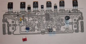
DONE at last !!
Woahhhh ! There actually was a lot to pack in there.
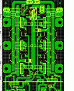
I was extreme in my layout of the circuit traces to what would actually be seen , (signal-wise). I am aiming for the least "cross contamination" between sections. 50mm separated by the rail trace should keep my input stage rather isolated from the bad, bad output inductor.
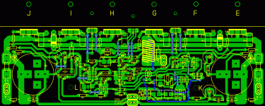
Below is the labeled PCB (attachment) , the .ZIP file has the BOM , schematic draft , and PCB draft. I have SPLAN , to make a "pretty" schematic , but would like to know whether there are any better cad's out there.
What shall we name it ?? (The amp)
Yes, center NFB takeoff I agree with. The close rail-trace/ wire twisting has been "demystified" - read this , --- Enduring Class B layout mythology ----
I've yet to see an OEM that runs parallel rail traces on a single amp PCB , although some HT amps run parallel copper bus bars to feed the 5-7 channels on one PCB , but adcom , luxman, nikko - just run the rails from each side. I have seen a silicon chip layout with the parallel traces , but no alternating (V+/V-/V+) output scheme. For diya's heatsinks (If I had 2) , I would of designed a flat- opposing OP 3-4 pair layout. BTW , none of those OEM's twist their wires.
OS
Woahhhh ! There actually was a lot to pack in there.
I was extreme in my layout of the circuit traces to what would actually be seen , (signal-wise). I am aiming for the least "cross contamination" between sections. 50mm separated by the rail trace should keep my input stage rather isolated from the bad, bad output inductor.
Below is the labeled PCB (attachment) , the .ZIP file has the BOM , schematic draft , and PCB draft. I have SPLAN , to make a "pretty" schematic , but would like to know whether there are any better cad's out there.
What shall we name it ?? (The amp)
Hi,
In my experience the Vcc and Vee entry points to the pcb should be kept as close as possible so that the supply wires can be twisted together. This will reduce EM radiation which is likely to swamp the distortion of the circuit.
Trust me, the routing of the power supply leads is absolutely critical. It is something that has to be seen to be believed. I only discovered it when I bought an AP520 and built a blameless amplifier (with my own pcb layout). The loop area between Vcc and Vee has to be kept as small as possible. Bob Cordell in his book, even advocated interspersing the output devices - N,P,N,P etc, in order to keep the area between the + and - supply tracks as small as possible.
I'm sorry if you already knew this, but as you are putting in so much effort, I thought I would mention it. Layout of psu wiring is and positioning of the power entry points on the pcb (and the associated tracking) is critical - as is the -ve feedback take off point (Self's book at least makes this point clear).
I hope this is of of some use,
Cheers, Ian
Yes, center NFB takeoff I agree with. The close rail-trace/ wire twisting has been "demystified" - read this , --- Enduring Class B layout mythology ----
I've yet to see an OEM that runs parallel rail traces on a single amp PCB , although some HT amps run parallel copper bus bars to feed the 5-7 channels on one PCB , but adcom , luxman, nikko - just run the rails from each side. I have seen a silicon chip layout with the parallel traces , but no alternating (V+/V-/V+) output scheme. For diya's heatsinks (If I had 2) , I would of designed a flat- opposing OP 3-4 pair layout. BTW , none of those OEM's twist their wires.
OS
Attachments
Great project, Pete!
A credit to you that you were chosen for this design.....
Good to see you using a nice EF2, proven front end.
DIYaudio rules!
Hugh
Woahhhh ! There actually was a lot to pack in there.
What shall we name it ?? (The amp)
OS
Boy, OS tore right through this! Proves he was the right guy for the job.
Maybe we should have a little naming contest with a set of boards as the prize...
Mark
Yes, center NFB takeoff I agree with. The close rail-trace/ wire twisting has been "demystified" - read this , --- Enduring Class B layout mythology ----
I've yet to see an OEM that runs parallel rail traces on a single amp PCB , although some HT amps run parallel copper bus bars to feed the 5-7 channels on one PCB , but adcom , luxman, nikko - just run the rails from each side. I have seen a silicon chip layout with the parallel traces , but no alternating (V+/V-/V+) output scheme. For diya's heatsinks (If I had 2) , I would of designed a flat- opposing OP 3-4 pair layout. BTW , none of those OEM's twist their wires.
OS
Thanks for the link. I maintain that it is still sensible to keep the supply loop area as small as possible, so that equal amounts of +ve and -ve currents are injected into sensitive areas. In my opinion, this is best achieved by having the psu entry points close together in the middle of the board, so that twisted supply cabling can be used.
Bob's post here - http://www.diyaudio.com/forums/soli...lls-power-amplifier-book-179.html#post2582005 sums up my views and agrees with my pratical experience with a distortion analyser.
Hi OS,
You may want to think about increasing the value of R25. As it stands, the collector current through Q9 at positive clipping will be rather large!
Regards,
Ian
I agree , carlos (DX) blew a few beta enhancer's here...
I only achieved a warm ksa992 with hours of clipping with 45v rails. 470R or more would not affect performance one bit.I segmented the whole design (below) ....
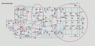
A=IPS - the "universal" input stage. You could omit/ jumper out the C-E of Q3/4, omit C6/R18-19 for the simple 2 device input pair. you could also not do this and use a low noise {ECB} input pair...
.. most of mouser's low Vceo- low noise to-92's (BC-xxx) are EBC.
(please comment on this !!! )
FET's are more problematic , some are "unobtainium" , have different DGS pinouts ..... it would be best to go the SOT23 way with a micro PCB. In this way, whatever BJT pads are chosen the SOT's can be routed (BF862 X2)
on the "micro PCB"
.B=The current sources , tried and true .... this will even minimize turn-on "thump". The real amps will stay 8.82ma VAS from 0C - 40C , no change.
C=VAS Changing R25 , no issue ... mje340/350 for Q10-12 , it will work. Jumper C8 - omit R24 , you have simple miller compensation. I also left capacitor pads on the negative feedback path for a little lead compensation (next to R6 on PCB) , i'll label it "LC".
D= The output stage , use anything
ON NJW/MJL x302/x281, Toshiba 5200/1943 - any 200w+ 200v+ 80Hfe + TO-264/TO-3p output device.Driver , the same MJE - 2sa/c - to-220.
I'm going to finalize the whole thing , right down to the mil spacing for the component leads , so I need a final comments on input pair or any other component choices. I tried to make it as DIY "friendly" as possible (larger pads , no special parts or form factors). Thanks ...
OS
Attachments
Thank you , Mark ...Boy, OS tore right through this! Proves he was the right guy for the job.
Maybe we should have a little naming contest with a set of boards as the prize...
Mark
But there are those small details to "sweat" now.
The reason for this thread.Visually , the board will be "pretty" (VERY visually appealing) and exactly 252 X 76 mm , the whole 25mm area above the output "line" (the E - J holes) will be gone , they were just for alignment.
I did this from "mind" ( no auto-routing) , for this is a "artform" (like a painting).
This has 99.999% chance of working the first time as it is , should we prototype it first ??
, as to not go down the road of the GOLDMUND , with all of it's mod's and shortcomings. BTW , that was not Alex MM's fault , they should of built it first - then went to production ( look at AKSA's latest fetzilla project).I will edit the BOM text to perfection , and write the "book" too. I have photo's of my AX , which is the first version of this amp ..exact same VAS/OP. Your call as to what format to do this in. PM me.
OS
Attachments
Last edited:
Member
Joined 2009
Paid Member
Visually , the board will be "pretty", for this is a "artform" (like a painting).
this is exactly the right approach

it has to be technically good, but that's just a ticket to enter the game, to be the best it has to look and feel like somebody really cared when it was designed.
Thanks for the link. I maintain that it is still sensible to keep the supply loop area as small as possible, so that equal amounts of +ve and -ve currents are injected into sensitive areas. In my opinion, this is best achieved by having the psu entry points close together in the middle of the board, so that twisted supply cabling can be used.
Bob's post here - http://www.diyaudio.com/forums/soli...lls-power-amplifier-book-179.html#post2582005 sums up my views and agrees with my pratical experience with a distortion analyser.
I agree that is slightly more ideal ,
Consider this - this amp has the supply onboard , rectified, unfiltered DC will be entering the fuses , no typical DC lines running from an external PS. The charging pulses will return to the main earth/CT near the edge of the board , the second set of thinner returns (CCS's/VAS/input ground's) will have far less "garbage' on them and shield the small signal area. This amps loop area is just 100mm total (C13/17 to the first outputs- 50mm X 2).
Now... with traces going down the PCB center , you would either have to jumper the circuit across the rails , or place most of the circuit on either side.
One would be a bad choice and one would waste real estate.
On another design (below) , it could be brought out one step further than what you see. Not only put the rails right together down the center , but split the P and N channel return traces to meet dead center at the end of the board.
I had to compromise for this application while still trying to retain the performance. My best guess , is that the amp will stay PPM up till 1/3 - 1/2 power , then slightly degrade to .005-.01%+ at high power levels/load. This is unavoidable with just the fact that we have a EF2.
This is why MY amp will be triple op / below layout. Not to say this will make a bit of difference in the sonics , but this also would be subjective. Lacking an AP , I did see the effect of loop area / cable inductance on the slew of a heavily loaded square wave on my present version of this amp.
OS
Attachments
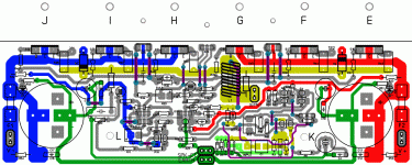
looking for BUGS....
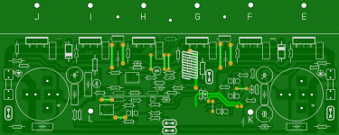
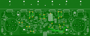
Voltages -( picture 1 ) and a real world layout (picture 2) .. this is the only way to push 99.999% to 100%. ps- red is V+, blue is V-, yellow= signal , greens are ground....
Still waiting for component/general suggestions before I "lock down" the design.
At $30-35 a pair (or whatever is the price) , I wish this was available when I started DIY.
OS
Attachments
- Home
- Amplifiers
- Solid State
- diyAB Amp - The "Honey Badger"