Fantastic work you're doing, SWF!
I think you are moving down the heady path to nirvana......
Your design approach is a subjective, informed one, and from where I stand there is no better way. Worry about the THD when you've finished.... you will probably find it's very low anyway.
If you can bias up the input stage so that the input blocking cap has more DC volts polarising it than AC throughput, then it will sound better. The reasons are not immediately obvious, but if you don't like this approach, you can always use a $75 teflon input cap. They definitely sound good....
If I had to choose between a low current mosfet, or DN2530, a pretty good one according to the datasheet, and a bipolar device, I would always choose the latter. Bipolars have high transconductance, they are cheap, they can be had in 250V ratings and higher, and they have tough bases which can stand all kinds of input abuse, unlike gates.
With a high Z fb network you will have quite a bit of thermal offset drift, since the Vbe of the VAS reduces with temp (around 1.8mV/C) and shows at the series fb resistor as a measureable drop, which transfers to the output as offset. For a NPN input stage and PNP VAS, you will have a rising offset as the VAS warms. By direct coupling the fb network without a DC blocker, as in Mike's design, your offset control will not be very good and servo may be the answer. No problem, you can do a servo with a zener, a couple of resistors, a transistor and a LED.
The acid test comes after listening to your amp on all kinds of music for two weeks. Does it image well? How noisy is it? Is the presentation musical? How about the bass? Is it 'warm' or 'cold'? How's the top end and midrange? etc etc, great material for OCD.
You have set the gain at 11. For a 25W amp, you should have a gain around 20 (26dB), as this will take it to full power with 707mVrms peak, close to the max for a CD player (though not a DVD). Going to around half this gain increase loop gain by almost 6dB, adds to stability issues.
IMHO it's best to keep VAS degeneration to the minimum, say no more than 47R, and stabilise the amp with a small miller cap and some phase lead. I would try 18pF and around 10pF of phase lead, from VAS collector to input stage fb node.
Then the amp should be able to drive anything, possibly even a 4" rusty nail....
Hugh
Mike, 200R of degeneration seems a lot. If the VAS runs at 11mA, then re is 26/11 = 2.3R. In my experience, ten times this resistance, near on 22R, is sufficient to swamp the non-linearities of this intrinsic emitter resistance, and further degeneration creates too much current variation in the first stage, detracting from its linearity due to Vbe/Vgs changes on the input device
Thanks for your feed back Hugh - As someone who never had an electronics lesson in his life I am aware that there are gaps in my knowledge so I have to confess I have no idea where your 26/11 calculation comes from. If 11 = mA what is the 26 ?
I wish I could build this thing now but until my things arrive form USA this is not possible so I am playing with this only in spice . . . but the extra degeneration in spice appears to bring only advantages - I will examin i/p stage current variation with different VAS degeneration for now and make & listen to this later.
However I think I can squeeze a jfet current source in there with only 50 ohms VAS degeneration
")
Last edited:
Mike.. have been looking at the JLH-amplifier and to me it looks like his DC-offset solution lies in the bottom.. you propose a current-source in top..any particular reason for that..??
In his diagram the solution is built into the CCS connected from the pos rail to the i/p device emitter.
In our ( reverse polarity ) design here, in it's current form the i/p stage does not have a connection from source to the the neg rail ( which I think is a very neat ) so as a starting point I just applied the principal that he uses which is that you add a similar device to the i/p device in a position where in tends to cancel the i/p device DC drift with temp.
How well it works in real life remains to be seen but I think it will be better that nothing ( and at the time swordfishy seemed to be looking for a bit more gain which this mod also provides )
mike
Mike,
The intrinsic emitter resistance of a bipolar device is 26/Ic, where Ic is the collector current in mA.
The 26 comes from the solid state physics formula behind this phenomenon and incorporates the Boltzman constant.
This implies that as the collector current increases, the Zout of a bipolar emitter drops assymptotically - a hyperbolic relationship which clearly is not linear.
Since the emitter degeneration resistor is in series with this intrinsic value, then it makes sense to 'linearise' the combination by swamping it with emitter degeneration.
I've only had a few lessons myself, wouldn't let that stop you.... probably means you don't know the limits and might even create something new!!
Hugh
Last edited:
Thx for the explanation Hugh.
I've been wondering about this area for quite while now. . .
. . . but as you say it's always good to check the theory with your ears.
I had SKA amps when I was in USA and they have something like 20 ohm emmiter degeneration resistors on the LTP which fits very well with this theory but for my ears the whole amp came to life and sounded generally better when I removed them - dynamics where so much better and I suspect this may be the issue swordfishy has run into - it's hard to judge dynamics in spice !
over & out
mike
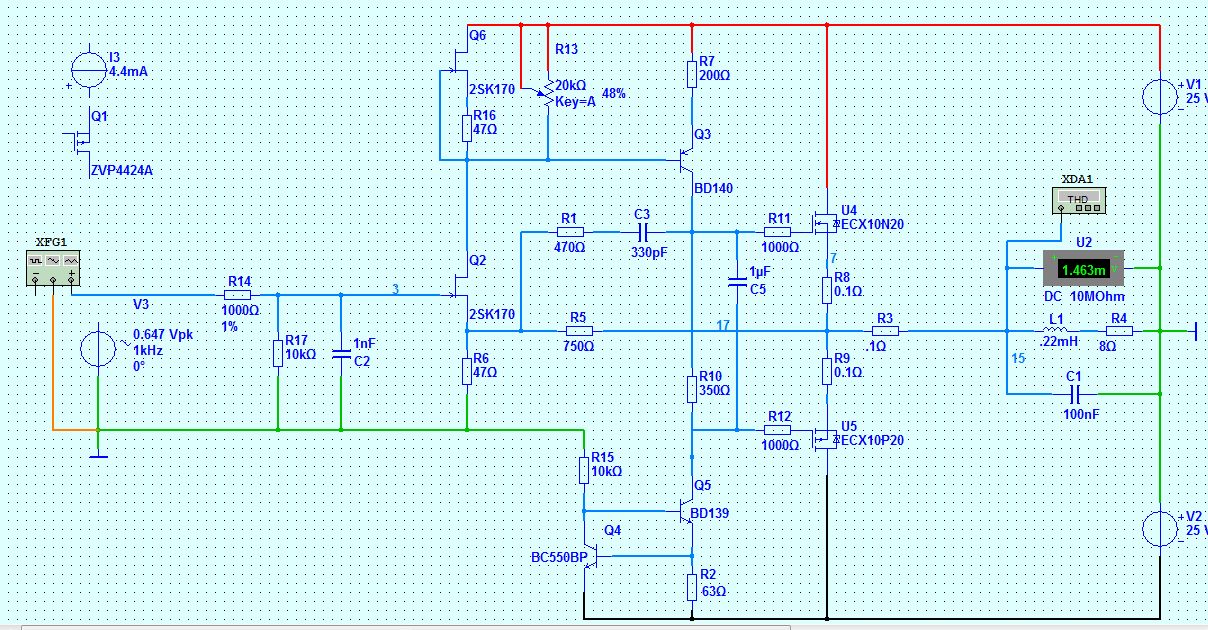
Not quite what I meant, mikelm.This measure lineup suggested may help a lot with DC offset on a DC linked version
See diagram below.
Where a JFET is used as a varible current source.
This replaces your potentiometer.
And this tweak does not help with DC-offset.
But it is a tweak for lowering the load of the input JFET and lower THD.
JFET will see a current source instead of a resistor, trimpot.
In fact this tweak may, for you, make DC-offset drift worse.
Better stick to your potentiometer and leave this tweak
to those that not use DC linked version.
Regards
Attachments
Dualism is good for process and advances of learning.
AKSA is a very welcome contributor.
Me Lineup has a different approach than AKSA.
I like to have lowest possible THD at any price, almost.
AKSA is not so much worried about ultralow THD.
He wants lower OLG and he wants possibly better sound.
While I go for anything that increase OLG open loop gain.
Is this situation bad?
No, it is good!!
It is in a dialogue between two standpoints
people get two sides and have better and broader chance to decide good.
It is in a dialogue we get a process. Process of learning.
I will learn as well.
Without AKSA, with his views and experiences
this topic would be more dead than alive.
The difference in his views forces us to think. To modify.
Now let us go on while this topic is still alive.
Regards
Lineup,
I appreciate your goodwill, and careful sponsorship of this thread. SWF is a 31 year old jumping out of his skin with different circuits and tweaks every hour of the day, hell, I was like that once... I see this as a learning exercise. His input is pivotal and much welcomed.
You correctly identify my approach, and fearlessly describe your own. Both approaches are valid and can learn from each other.
However, the low THD approach is the conventional engineering focus and has been with us for decades. Sometimes it works, sometimes it doesn't. Often very low THD amps - the Self Blameless for example - don't really appeal in a long listening session for most audiophiles. Tastes vary. The purists, often designers, will say that they want a straight wire with gain, the amp should add nothing at all. But the majority of audiophiles, it seems to me, often with little or no knowledge of the circuitry, don't seem to like the straight wire with gain, many of them drifting across to the highly coloured tube school of audio. We can sweep aside their assessment by saying human perception is unreliable, tastes vary, people wouldn't know a good amp if it bit them on the nose, and so on. But you will find a lot of knowledgeable, thoughtful people saying that you should never buy anything without listening to it carefully, with music you know well. I second that. After all, our food, clothing, artistic and entertainment preferences are formed over a long time, and until we hear/see/smell/touch something a few hundred times, we really don't know the experience well enough to form a preference.
Therefore, we might be measuring the wrong thing, trying to assess how fast the automobile can go by reading off the licence plate....
My thoughts are that the profile of the distortion is important. For example, if the distortion is 0.05%, a highish figure, but 99% of it is H2 and H4, it will probably sound rather better than 0.005% where 80% of it is H5 and H7. Jean Hiraga first noted this in the sixties. Earl Geddes with his Gedlee Index has formalised this observation, and takes weighted, high account of odd order distortion artefacts. Absolutely nothing is new under the sun.
Furthermore, lots of loop gain means that while the distortion artefacts, taken individually, are reduced in amplitude, they increase in number, and trail on until at least the 25th harmonic, particularly beyond a loop gain of about 40dB. Could it be that if we keep loop gain below about 45dB we might have better sound?
Lastly, the back emf and load phase shift of a speaker is a truly malevolent thing, and it seriously disrupts the feedback mechanism, causing correction to be phase shifted radically from the input. This confuses the amp, which cannot distinguish between its distortion/phase shift and that of the speaker to which it is corrected. You could argue this is the idea, but there is no doubt that the reactive speaker load seriously destabilises amplifiers. Again, this problem is ameliorated by reducing loop gain.
Hugh
Me Lineup has a different . . ..
I like to have lowest possible THD at any price . . .
. . . I go for anything that increase OLG open loop gain.
Ah, then I think you may like this variation
@ 10V in 8ohm this essentially has no distortion
and it seems stable into tricky loads also
enjoy
p.s. I did not put variable resistor in CCS on purpose. I have strong views about resistors - I think most of them sound horrible and variable ones sound even worse so I prefer to have dominant current via a fixed resistor
Attachments
How did you do that?Ah, then I think you may like this variation
@ 10V in 8ohm this essentially has no distortion
and it seems stable into tricky loads also
enjoy
Have you got a prototype with loudspeaker?
Or are you refering to a SPICE run?
. . . but I did notice that my spice square wave ringing & swordfishy's real world square wave ringing with varying capacitive loads were very similar which is quite encouraging.
Meanwhile, Swordfishy appears to have gone to sleep and left us all hanging here to see his final circuits . . .
Meanwhile, Swordfishy appears to have gone to sleep and left us all hanging here to see his final circuits . . .
That's what I did and with a 1k ohm & 1nF i/p filter this high OLG version works just fine
Using cascoded BJT's gives about 25db less OLG at 4meghz than using a mosfet VAS so in comparison stabilisation is fairly easy.
Anyway, I have the feeling that I have posted enough spicing on this now. Now I will wait till I actually build.
Using cascoded BJT's gives about 25db less OLG at 4meghz than using a mosfet VAS so in comparison stabilisation is fairly easy.
Anyway, I have the feeling that I have posted enough spicing on this now. Now I will wait till I actually build.
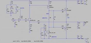
This is it!
All,
I present to to you, the ultimate, the best, the penultimate. It does not get any better. Take every good comment I have made about sound, add them together and you get this.
Not what you expected me to post huh? Thanks to lineup for coming up with almost the exact circuit without even lifting a soldering iron. And to Hugh for the CCS and DC offset tweak. This is it.
I move on to PCBs now. I see no need to experiment further, except maybe to find a better FET for the VAS.
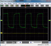
Stable? Check out the 20kHz square wave....the best yet.
I will post the long story about how I got here tomorrow. It is all about OLG. The JFET does not have enough so we needed more from the VAS. Mikelm, I bet you're rolling your eyes now aren't you
Edit: oops, please ignore the "NMOS" text...it is of course a P channel device.
All,
I present to to you, the ultimate, the best, the penultimate. It does not get any better. Take every good comment I have made about sound, add them together and you get this.
Not what you expected me to post huh? Thanks to lineup for coming up with almost the exact circuit without even lifting a soldering iron. And to Hugh for the CCS and DC offset tweak. This is it.
I move on to PCBs now. I see no need to experiment further, except maybe to find a better FET for the VAS.
Stable? Check out the 20kHz square wave....the best yet.
I will post the long story about how I got here tomorrow. It is all about OLG. The JFET does not have enough so we needed more from the VAS. Mikelm, I bet you're rolling your eyes now aren't you
Edit: oops, please ignore the "NMOS" text...it is of course a P channel device.
Attachments
Last edited:
SWF,
Congratulations - this looks damn good. Excellent 20KHz square wave too....
Do you know loop gain? With low gm 1st stage, and high gain VAS, I'd think around 60dB? Nice CLG, too, no less than 26, very nice, around 28.3dB.
So I'd estimate about 6mA in the input stage? That's 150mW dissipation in the jfet, within ratings. Should be reliable.
That's a very big VAS current, particularly for laterals, and a mosfet with 51R of degeneration, no miller cap! WOW!! What is the voltage across R8, Greg?
And only half an amp of quiescent - that's 25W of heat, manageable, only 12.5W per device, that's about 4W in Class A, AB from then on. Where does it clip? Symmetrical?
Finally, a good 2V or more across C1. Input of C1 should have a ground ref resistor, I'd say around 220k.
Brilliant, Greg, would you like my input with the pcb?
Cheers,
Hugh
Last edited:
- Status
- This old topic is closed. If you want to reopen this topic, contact a moderator using the "Report Post" button.
- Home
- Amplifiers
- Solid State
- JFET input, MOSFET VAS, LATERAL output = Perfect!!